


 The Right Approach: The Pros and Cons of PCB Vertical Integration
 American Made Advocacy: PCBAA’s Fifth Annual Meeting—Growing Membership and Valuable Relationships
 It's Only Common Sense: Why the Best Years of Electronics Are Still Ahead of Us


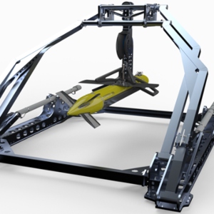
Kraken Robotics Inc., Canada’s Ocean Company, is very pleased to announce that it has signed a contract with Danish Ministry of Defence, Acquisition and Logistics Organization (DALO) to supply mine-hunting sonar equipment to the Royal Danish Navy. This was a competitive bid process and under the program, Kraken will deliver its KATFISH™ towed Synthetic Aperture Sonar, Tentacle® Winch and Autonomous Launch and Recovery System (ALARS). Kraken’s minehunting system will be integrated onboard the Royal Danish Navy’s optionally unmanned surface vessels (MSFs as seen in Figure 3). The total contract value is approximately $36 million, with the majority of that received over a 2-year equipment acquisition phase. Product margins on this contract are expected to be in line with historical Kraken averages.
Karl Kenny, Kraken President and CEO noted: “We are very pleased to sign this contract to supply our KATFISH™ and ALARS systems to the Royal Danish Navy. This was a very competitive process and we are proud to have been selected. We are looking forward to a long-term relationship with the Danish Navy. As part of its commitment to Denmark, Kraken will be expanding its European presence with the establishment of a new Danish Centre of Excellence in Mine Counter Measures. This new operation will not only conduct research and development to further improve the capabilities of Kraken’s world-class MCM solutions but will also be able to offer local technical support for Danish customers. Kraken’s new Danish operation will also engage with local Danish companies, universities and technical institutes, ensuring a long term benefit to Danish technical development.”
The Head of the Maritime Division within DALO, Captain (RDN) Kim Bo Meier noted:
“The ability to recognize conditions below sea level on Danish maritime territory is as ever considered a vital task of the Royal Danish Navy and its MCM forces. After a lengthy and rigorous procurement process the Royal Danish Navy has selected Kraken’s KATFISH™ 180 system as its future main mine hunting sensor. A modern sensor, which within the months to come is to be fully integrated in to the Danish MCM modular concept of unmanned and remotely controlled MCM drones. With this new sensor the Royal Danish Navy can maintain its MCM capacity and necessary operational preparedness in relation to being able to locate and clear mines in both national and international waters and straits. We look forward cooperating with Kraken ensuring a smooth integration of the new main sensor.”


