-
- News
- Books
Featured Books
- smt007 Magazine
Latest Issues
Current IssueDo You Have X-ray Vision?
Has X-ray’s time finally come in electronics manufacturing? Join us in this issue of SMT007 Magazine, where we answer this question and others to bring more efficiency to your bottom line.
IPC APEX EXPO 2025: A Preview
It’s that time again. If you’re going to Anaheim for IPC APEX EXPO 2025, we’ll see you there. In the meantime, consider this issue of SMT007 Magazine to be your golden ticket to planning the show.
Technical Resources
Key industry organizations–all with knowledge sharing as a part of their mission–share their technical repositories in this issue of SMT007 Magazine. Where can you find information critical to your work? Odds are, right here.
- Articles
- Columns
Search Console
- Links
- Media kit
||| MENU - smt007 Magazine
National Circuit Assembly Offers Authentic Measurement and Inspection with New 3D SPI System
September 18, 2020 | National Circuit AssemblyEstimated reading time: Less than a minute

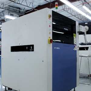
National Circuit Assembly, a provider of PCB, cable and electro/mechanical manufacturing and test services to leading OEMs, has purchased and installed a PARMI HS60L 3D Solder Paste Inspection (SPI) system. With the most reliable and accurate 3D data, NCA offers reliable, accurate inspection.
“Introducing this automated SPI machine into our production lines will have a tremendous impact on our efficiency and quality control,” says Eric Nguyen, NCA VP Manufacturing. “Rather than relying on possible human error to inspect the quality of our solder paste placement, we can lower lead times and promise higher success rates across the board through a more accurate, automated process.”
PARMI’s intelligent vision algorithm applied to the high-quality 3D data detects every type of solder paste defect, which translates to zero false calls for NCA. The measurable items are height, area, volume and positional offset that deviate from tolerance limits.
The remarkable design concept of the HS60L, including rotating laser sheet beam against the scan direction and maintaining the small angle between the laser sheet beam and camera optical axis, ensures high performance, repeatability and accuracy.
Suggested Items
KYZEN to Highlight Stencil and Cleaning Solutions at SMTA Monterrey
03/27/2025 | KYZEN'KYZEN, the global leader in innovative environmentally friendly cleaning chemistries, will exhibit at the SMTA Monterrey Expo & Tech Forum scheduled to take place on Thursday, April 10 at the Cintermex Convention Center in Monterrey, Nuevo León. KYZEN cleaning experts will be on-site highlighting stencil cleaning chemistries KYZEN E5631J and CYBERSOLV C8882.
Indium to Showcase Proven EV Products and High-Reliability Alloys at Productronica China
03/26/2025 | Indium CorporationAs a global materials supplier and trusted partner in electric vehicle (EV) and e-Mobility manufacturing, Indium Corporation® is proud to showcase its high-reliability alloys and soldering solutions at Productronica China, March 26-28, in Shanghai, China.
SolderKing Enhances Brainboxes' Electronics Manufacturing with Expert Support and Advanced Materials
03/26/2025 | SolderKingIn modern electronics manufacturing, success relies on more than high-quality soldering materials. Technical knowledge and process expertise are just as crucial for achieving consistent results. SolderKing, a leading UK manufacturer, provides both, combining advanced consumables with specialist support to help manufacturers optimise their soldering processes.
AIM to Highlight Type 5 Solder and Other Leading Products at SMTA Monterrey Expo & Tech Forum
03/20/2025 | AIM SolderAIM Solder, a leading global manufacturer of solder assembly materials for the electronics industry, is pleased to announce its participation in the upcoming SMTA Monterrey Expo & Tech Forum taking place on April 10 at Cintermex in Monterrey, Nuevo Leon, Mexico.
Hentec Industries/RPS Automation to Showcase Valence 2508 at IPC Expo 2025
03/17/2025 | Hentec Industries/RPS AutomationThe Valence 2508 Selective Soldering System is engineered for high-mix, high-volume, advanced PCB production. It supports boards ranging from 25 x 25 mm to 559 x 559 mm (1 x 1 in. to 22 x 22 in.), with a maximum processing area of 508 x 508 mm (20 x 20 in.).