-

- News
- Books
Featured Books
- smt007 Magazine
Latest Issues
Current Issue
What's Your Sweet Spot?
Are you in a niche that’s growing or shrinking? Is it time to reassess and refocus? We spotlight companies thriving by redefining or reinforcing their niche. What are their insights?

Moving Forward With Confidence
In this issue, we focus on sales and quoting, workforce training, new IPC leadership in the U.S. and Canada, the effects of tariffs, CFX standards, and much more—all designed to provide perspective as you move through the cloud bank of today's shifting economic market.

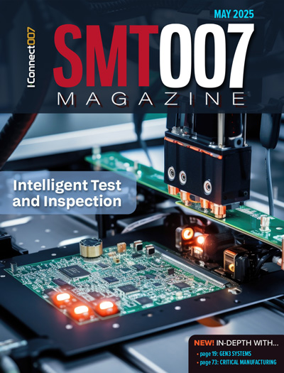
Intelligent Test and Inspection
Are you ready to explore the cutting-edge advancements shaping the electronics manufacturing industry? The May 2025 issue of SMT007 Magazine is packed with insights, innovations, and expert perspectives that you won’t want to miss.
- Articles
- Columns
- Links
- Media kit
||| MENU - smt007 Magazine
90% Solder Dross Recovery: Eliminate Waste, Save Money
October 20, 2020 | Nolan Johnson, I-Connect007Estimated reading time: 2 minutes
The impact of 90% solder dross recovery can have a substantial impact on reducing waste and increasing cost savings. I recently spoke with Jay Hardin, MS2® product manager at P. Kay Metal, about the process and benefits of efficient solder dross recovery, as well as product roadmaps, the soldering machine market, and raw materials supply chain for solder alloy manufacturing. As Jay says, “For many companies, the savings are in the thousands or millions” of dollars.
Nolan Johnson: Hi, Jay. Could you tell us a little about yourself and P. Kay Metal?
Jay Hardin: I’m with P. Kay Metal, Inc., headquartered out of Los Angeles, California. I’m the product manager for the company. Since 1978, we’ve been a tin-lead alloy and chemical manufacturer, which includes fluxes and our specialty product called MS2.
Johnson: With a product mix like that, do you primarily sell into both fabrication and assembly?
Hardin: Yes. Primary customers are based in Mexico and the Western United States. The specialty product, MS2, became a global product in 2006. It has been used by most major contract manufacturers and assemblers in the world, including the largest ones. We have contracts with many of the facilities around the world and can supply them all from our headquarters in Los Angeles.
Johnson: The MS2 product is a little different. Can you explain MS2 and what it does?
Hardin: Our company is a solder manufacturer, but our history has always been in dross recycling. Solder dross is a waste that’s formed in the through-hole assembly process of PCB manufacturing—a large solder pot of the solder is constantly in motion, forming a gum called dross, which is removed from the process and sold back to companies like us. We recycle that solder dross back to usable metal and can then sell it back to the customer. The MS2 product was developed when everything was becoming lead-free, and prices of solder went from being $2 a pound to up to $30 a pound. The cost of dross became a huge problem once everything went lead-free.
We thought that the product we used to recycle solder dross could be re-blended and, in a pure form, sold to the producers of the dross globally to eliminate both the solder dross problem and cost. The solder dross that customers generate from the wave soldering machines represents about 60–80% of the total waste that they generate in their facility. It also requires them to purchase new solder bars. About 80% of the new solder bars that a customer buys is to replace the solder dross that they’re removing from the process. If we’re able to eliminate that waste and help the customer to become 95+% efficient with the solder they buy, all they have to do is implement the MS2 process into their lines.
To read this entire interview, which appeared in the September 2020 issue of SMT007 Magazine, click here.
Suggested Items
Driving Innovation: Direct Imaging vs. Conventional Exposure
07/01/2025 | Simon Khesin -- Column: Driving InnovationMy first camera used Kodak film. I even experimented with developing photos in the bathroom, though I usually dropped the film off at a Kodak center and received the prints two weeks later, only to discover that some images were out of focus or poorly framed. Today, every smartphone contains a high-quality camera capable of producing stunning images instantly.
Hands-On Demos Now Available for Apollo Seiko’s EF and AF Selective Soldering Lines
06/30/2025 | Apollo SeikoApollo Seiko, a leading innovator in soldering technology, is excited to spotlight its expanded lineup of EF and AF Series Selective Soldering Systems, now available for live demonstrations in its newly dedicated demo room.
Indium Corporation Expert to Present on Automotive and Industrial Solder Bonding Solutions at Global Electronics Association Workshop
06/26/2025 | IndiumIndium Corporation Principal Engineer, Advanced Materials, Andy Mackie, Ph.D., MSc, will deliver a technical presentation on innovative solder bonding solutions for automotive and industrial applications at the Global Electronics A
Fresh PCB Concepts: Assembly Challenges with Micro Components and Standard Solder Mask Practices
06/26/2025 | Team NCAB -- Column: Fresh PCB ConceptsMicro components have redefined what is possible in PCB design. With package sizes like 01005 and 0201 becoming more common in high-density layouts, designers are now expected to pack more performance into smaller spaces than ever before. While these advancements support miniaturization and functionality, they introduce new assembly challenges, particularly with traditional solder mask and legend application processes.
Knocking Down the Bone Pile: Tin Whisker Mitigation in Aerospace Applications, Part 3
06/25/2025 | Nash Bell -- Column: Knocking Down the Bone PileTin whiskers are slender, hair-like metallic growths that can develop on the surface of tin-plated electronic components. Typically measuring a few micrometers in diameter and growing several millimeters in length, they form through an electrochemical process influenced by environmental factors such as temperature variations, mechanical or compressive stress, and the aging of solder alloys.


