


 The Marketing Minute: If Your Marketing Budget Gets Cut in Half, Then What?
 Punching Out: How Are the Big Boys in Electronics Doing?
 It’s Only Common Sense: Complexity Is the Enemy of Profit


Plasmatreat Releases Surface Cleaning for a Reliable Wire Bonding Process
October 28, 2020 | PlasmatreatEstimated reading time: 2 minutes
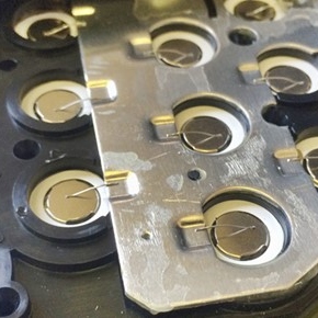
Openair-Plasma from Plasmatreat GmbH is one of the leading technologies worldwide to activate and clean surfaces. It is used in numerous applications to pretreat different substrates. It can also be used to clean metal surfaces for solid wire bonding. The Openair-Plasma technology is a cost-efficient process and can be integrated inline, allowing the bonding process to take place directly after the cleaning is completed.
"Metal can be cleaned using three processes which have different effects and have different treatment goals," says Nico Coenen, Global Business Development Manager Electronics Market of Plasmatreat GmbH, explaining the basic possibilities of plasma treatment. The first process, neutralization, involves the removal of both surface charge and statically bound dirt such as dust particles. This is done by the charge carriers of the Openair-Plasma treatment. In the second process, the volatile components such as moisture and VOCs (volatile organic compounds) are eliminated by evaporation through the thermal effect of the Openair-Plasma treatment. The final cleaning process is removing organic contaminants. The reactive nature of Openair-Plasma causes hydrocarbon chains to be broken down and split into smaller, volatile molecules (up to H2O and CO2).
The successful treatment can be verified, for example, by using an atomic force microscope, which provides visual evidence of the change in the surface. This is a special scanning probe microscope which is used in surface chemistry for mechanical scanning of surfaces and for measuring atomic forces on the nanometer scale. Furthermore, the contact angle method can be used to prove the modified surface tension e.g. by a drop of water. The water drop on the plasma-treated surface changes its wetting properties in such a way that the contact angle and height are reduced and the surface is becoming more hydrophilic.
This is the result of surface cleaning with Openair-Plasma. Especially oxide surfaces, but also contamination caused by bleed out, interfere with the bonding process and prevent reliable connections. Openair-Plasma removes both surface contamination and the oxide layer and the clean surface of the metal alloy is revealed. This is beneficial, in semiconductor applications as particularly clean surfaces are required here in order to reliably bond the ultra-fine wires. The plasma-treated surface allows bonded materials to form a more stable and larger-area connection.
A similar process is used to remove copper oxides, especially in semiconductor and LED applications. By using X-ray photoelectron spectroscopy, the chemical composition of solids and their surface can be determined without causing damage. After treating copper, it can therefore be determined that the surface proportion of copper increases from 3% to 38%, with a concomitant reduction in the carbon content from 43% to 18%. "These changes clearly show that the copper oxide has been reduced and the copper surface area increased," says Coenen. The contact angle analysis also shows a comparable result. Bond wires therefore also form reliable connections here.
In addition to aluminum and copper substrates, nickel surfaces show similarly good properties after being treated with Openair-Plasma. This is particularly important in battery production. Since nickel oxide acts like a barrier layer, which massively complicates the connection with other materials, the cleaning of the nickel surface from oxides is essential. Plasmatreat has therefore developed a special jet for this application that matches the general requirements and at the same time meets the temperature requirements of the process step, for example does not exceed the limit of 50° Celsius.
"The degree to which the individual substrates allow stable wire bonding depends on the material in use. However, the upstream plasma surface treatment improves the application window of the wire bonding process in any case. Both wettability and adhesion are optimized," says Coenen.
Share on:


Testimonial
"Advertising in PCB007 Magazine has been a great way to showcase our bare board testers to the right audience. The I-Connect007 team makes the process smooth and professional. We’re proud to be featured in such a trusted publication."
Klaus Koziol - atgSuggested Items
I-Connect007 Releases The Printed Circuit Designer’s Guide to… Direct Metallization: A Guide to Complex PCB Fabrication
05/13/2026 | I-Connect007As PCB complexity continues to accelerate, fabricators and OEMs are reevaluating long-standing manufacturing processes to meet the demands of AI, HDI, advanced packaging, and next-generation electronics. To address these evolving challenges, I-Connect007 is proud to announce the release of The Printed Circuit Designer’s Guide to… Direct Metallization: A Guide to Complex PCB Fabrication, authored by MacDermid Alpha Solution’s Carmichael Gugliotti.
Driving Innovation: Selecting the Right Laser Source
04/28/2026 | Simon Khesin -- Column: Driving InnovationWhen I first joined Schmoll Maschinen, I brought experience from almost every PCB process, except for laser. As I immersed myself in laser processing, I realized why it can seem so daunting to a newcomer. The complexity arises from three intersecting factors: A vast variety of laser sources: CO2, UV-nano, green-pico, UV-pico, IR-pico, and others; a diverse range of applications: Drilling, cutting, ablation, and more; and an extensive list of materials: These have vastly different absorption rates. Choosing the right machine or laser source is rarely trivial. Even for experienced engineers, answering "Which source is best?" requires examining the business's specific goals.
Institute of Circuit Technology Spring Seminar 2026: A Bright Future in Europe
04/23/2026 | Pete Starkey, I-Connect007Through the leafy lanes and spring flowers of Warwickshire and back to Meridan, the traditional centre of England, and now officially part of the Metropolitan Borough of Solihull in the county of the West Midlands, I attended the Annual General Meeting and Spring Seminar of the Institute of Circuit Technology (ICT) on April 14. Out of the AGM came notable changes in leadership at the top of the Institute: the retirement of Mat Beadel as chair and Emma Hudson as technical director. Effective May 1, Steve Driver is the new chair, and Alun Morgan is the new technical director.
ACCM Unveils Negative and Near-zero CTE Materials for Large-Format AI Chips
04/21/2026 | Advanced Chip and Circuit MaterialsAdvanced Chip and Circuit Materials, Inc. (ACCM) has launched two new materials: Celeritas HM50, with a negative coefficient of thermal expansion (CTE) of -8 ppm/°C to offset the positive CTE and expansion of copper with temperature on circuit boards, and Celeritas HM001, with near-zero CTE and the low-loss performance needed for high-speed signal layers to 224 Gb/s and faster in artificial intelligence (AI) circuits.
Fresh PCB Concepts: Designing PCBs for Harsh Environments—Reliability Is Engineered Upstream
04/23/2026 | Team NCAB -- Column: Fresh PCB ConceptsWhen engineers hear the phrase “harsh environment,” they usually think of the extreme temperature swings, vibration and shock, pressure changes, or radiation in aerospace. However, aerospace is not the only harsh environment where electronic assemblies must survive. Automotive power electronics, downhole oil and gas tools, marine controls, rail systems, defense platforms, and industrial automation equipment all expose PCBs to environments that are equally unforgiving. The stress mechanisms may differ, but the physics does not.