-

- News
- Books
Featured Books
- smt007 Magazine
Latest Issues
Current Issue
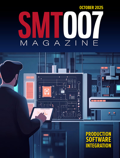
Production Software Integration
EMS companies need advanced software systems to thrive and compete. But these systems require significant effort to integrate and deploy. What is the reality, and how can we make it easier for everyone?

Spotlight on India
We invite you on a virtual tour of India’s thriving ecosystem, guided by the Global Electronics Association’s India office staff, who share their insights into the region’s growth and opportunities.

Supply Chain Strategies
A successful brand is built on strong customer relationships—anchored by a well-orchestrated supply chain at its core. This month, we look at how managing your supply chain directly influences customer perception.
- Articles
- Columns
- Links
- Media kit
||| MENU - smt007 Magazine
CyberOptics to Present ‘Metrology and Inspection’ Paper at Virtual IEEE PAINE Conference
November 18, 2020 | CyberOptics CorporationEstimated reading time: 2 minutes
CyberOptics® Corporation, a leading global developer and manufacturer of high-precision 3D sensing technology solutions, will present at the Virtual IEEE International Conference on Physical Assurance and Inspection of Electronics (PAINE) on December 16th at 8:00amCT.
Tim Skunes, VP of R&D at CyberOptics, will share the technical presentation ‘Fast, 100% 3D Wafer Bump Metrology and Inspection to Improve Yields and 3D System Integration’ at the IEEE PAINE Conference.
Advanced Packaging (AP) and wafer level packaging (WLP) continue to be among the most dynamic and rapidly evolving areas of semiconductor development and manufacturing. Most of these new processes take advantage of the third dimension, going vertical to continue packing more computing power into less space while circumventing the difficulties posed by further reductions in two-dimensional size.
As the processes and features they create have become smaller and more complex, manufacturers face an increasing need for high-precision inspection and measurement to detect defects and improve process control. This need is amplified by the fact that these processes use expensive known good die, making the cost of failure extremely high. Bump metrology is fundamentally three-dimensional and bump height is just as important as size and location. Controlling bump height, both absolute and relative to neighboring bumps (coplanarity), is critical to ensuring good, reliable connections between stacked components.
Multiple Reflection Suppression™ (MRS™) sensor technology addresses this challenge by comparing data from multiple perspectives and fringe frequencies to identify and reject these spurious signals. The sensor’s unique optical architecture and the system’s proprietary image fusing and processing algorithms provide accurate 3D characterization that is several times faster than conventional PSP. MRS sensor technology in the SQ3000™ Multi-Function System has been widely adopted for high-precision inspection and metrology for surface mount technology (SMT) and semiconductor applications. The NanoResolution MRS sensor has been developed specifically for AP and WLP applications to improve yields and process control.
The MRS sensor integrated into CyberOptics’ WX3000™ system provides sub-micrometer accuracy on features as small as 25µm. While retaining its ability to reject spurious multiple reflections, it adds the ability to capture and analyze specular reflections from shiny surfaces of solder balls, bumps and pillars, allowing accurate inspection and 3D metrology of these critical packaging features. The MRS sensor is 2-3X faster than alternative technologies. With data processing speeds in excess of 75 million 3D points per second, it delivers production-worthy throughput greater than 25 wafers (300mm) per hour. Both 3D/2D data is attained at the same time vs. time-consuming alternative methods that require separate scans for 3D and 2D. Complete 100% 3D/2D inspection can be accomplished at high speed for bump metrology, as compared to a sampling approach.
Testimonial
"We’re proud to call I-Connect007 a trusted partner. Their innovative approach and industry insight made our podcast collaboration a success by connecting us with the right audience and delivering real results."
Julia McCaffrey - NCAB GroupSuggested Items
Rehm Wins Mexico Technology Award for CondensoXLine with Formic Acid
10/17/2025 | Rehm Thermal SystemsModern electronics manufacturing requires technologies with high reliability. By using formic acid in convection, condensation, and contact soldering, Rehm Thermal Systems’ equipment ensures reliable, void-free solder joints — even when using flux-free solder pastes.
Indium Experts to Deliver Technical Presentations at SMTA International
10/14/2025 | Indium CorporationAs one of the leading materials providers to the power electronics assembly industry, Indium Corporation experts will share their technical insight on a wide range of innovative solder solutions at SMTA International (SMTAI), to be held October 19-23 in Rosemont, Illinois.
Knocking Down the Bone Pile: Revamp Your Components with BGA Reballing
10/14/2025 | Nash Bell -- Column: Knocking Down the Bone PileBall grid array (BGA) components evolved from pin grid array (PGA) devices, carrying over many of the same electrical benefits while introducing a more compact and efficient interconnect format. Instead of discrete leads, BGAs rely on solder balls on the underside of the package to connect to the PCB. In some advanced designs, solder balls are on both the PCB and the BGA package. In stacked configurations, such as package-on-package (PoP), these solder balls also interconnect multiple packages, enabling higher functionality in a smaller footprint.
Indium to Showcase High-Reliability Solder and Flux-Cored Wire Solutions at SMTA International
10/09/2025 | Indium CorporationAs one of the leading materials providers in the electronics industry, Indium Corporation® will feature its innovative, high-reliability solder and flux-cored wire products at SMTA International (SMTAI), to be held October 19-23 in Rosemont, Illinois.
‘Create your Connections’ – Rehm at productronica 2025 in Munich
10/08/2025 | Rehm Thermal SystemsThe electronics industry is undergoing dynamic transformation: smart production lines, sustainability, artificial intelligence, and sensor technologies dominate current discussions.


