


 The Marketing Minute: If Your Marketing Budget Gets Cut in Half, Then What?
 Punching Out: How Are the Big Boys in Electronics Doing?
 It’s Only Common Sense: Complexity Is the Enemy of Profit


Würth Elektronik Switching to More Sustainable Packaging
November 27, 2020 | Wurth ElektronikEstimated reading time: 1 minute
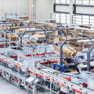
Logistics at one of Europe’s biggest manufacturers of electronic and electromechanical components has declared war on packaging waste. Würth Elektronik is putting all goods packaging processes to the test. The internal goals: drastic reduction of plastics and a switch to more sustainable materials.
Many waste-reducing measures have already been realized or are being implemented: For example, Würth Elektronik's Logistics only uses filling material based on recycled paper and also minimizes consumption by using hold-down devices and separating boxes. Padded envelopes are plastic-free, paper-based parcel tape holds parcels together where necessary, and boxes with lids save on adhesive tape. Plastic bags are being replaced by parchment paper bags on a large scale, for example for the delivery documents on the outside of parcels.
On the occasion of the European Week for Waste Reduction (Nov. 21-29, 2020) says Georgios Stamos, Head of Logistics in Waldenburg, Environmental Officer in Logistics at Würth Elektronik eiSos: "According to the German Federal Environment Agency, per capita packaging consumption has increased by 17.9 percent since 2010. Of this, more than half is caused by industry and commerce. So we are looking closely where we can become more sustainable. We are currently evaluating cardboard boxes that consist of up to 50 percent grass. In doing so, we are facing up to special requirements: Because we, as a developer service provider, offer free samples and design kits with replenishment, and this makes for a large number of small shipments. This service should be maintained, of course, but will be provided more sustainably in the future. Both here and elsewhere, protecting our environment involves a multitude of coordinated steps, which come with costs for the company. But the reduction of packaging waste is a responsibility that we as the workforce and company are happy to accept with great commitment.”
Share on:


Testimonial
"We’re proud to call I-Connect007 a trusted partner. Their innovative approach and industry insight made our podcast collaboration a success by connecting us with the right audience and delivering real results."
Julia McCaffrey - NCAB GroupSuggested Items
What Heterogeneous Integration Means for EMS Providers
05/14/2026 | Nolan Johnson, I-Connect007Dr. Ravi Mahajan, an Intel Fellow and Director of Intel’s Technology and Pathfinding group, delivered a keynote at the APEX EXPO 2026 technical conference on using heterogeneous integration (HI) as a strategy and on how advanced packaging technology serves as the technical apex for implementing that strategy. Mahajan’s previous papers and industry presentations on such topics as interconnect density, signal integrity, power delivery, thermal path, and assembly yield as system-level constraints confirm him as an expert on package optimization.
System Architecture Beyond the Die With Advanced Packaging as the Scaling Factor
05/14/2026 | Chetan Arvind Patil, Marvell TechnologyIn conventional monolithic semiconductor design, system integration was achieved within a single die and constrained by reticle limits. Compute cores, cache, memory controllers, and input output (I/O) interfaces were all co-optimized on a single process node, with performance closely tied to transistor density and on-die interconnect efficiency. This monolithic system-on-chip (SoC) approach enabled low-latency communication and relatively straightforward power delivery. However, as design for compute-intensive SoCs approaches reticle limits and advanced-node costs increase, the ability to continue scaling within a single die begins to diminish.
I-Connect007 Announces Upcoming Issue of Advanced Electronics Packaging Digest
05/13/2026 | I-Connect007The next issue of Advanced Electronics Packaging Digest examines the materials, architectures, and integration strategies shaping the next phase of electronics innovation, from reinforcement materials under thermal and frequency pressure to heterogeneous integration and advanced packaging as a system-level scaling factor.
ASE, WUS Announce Strategic Collaboration to Build Advanced AI Packaging Hub in Kaohsiung
05/08/2026 | ASE GroupAdvanced Semiconductor Engineering, Inc. (ASE) and WUS Printed Circuit Co., Ltd. (WUS) announced today a strategic collaboration for the construction of a state-of-the-art manufacturing facility in the Nanzih Technology Industrial Park, Kaohsiung.
SEMI 3D & Systems Summit to Advance AI, Hybrid Bonding, and Chiplet Ecosystem
05/06/2026 | SEMIGlobal experts in advanced semiconductor packaging and 3D integration will convene at the annual SEMI 3D & Systems Summit, June 17–19, 2026, in Dresden, Germany.