


 The Marketing Minute: If Your Marketing Budget Gets Cut in Half, Then What?
 Punching Out: How Are the Big Boys in Electronics Doing?
 It’s Only Common Sense: Complexity Is the Enemy of Profit


LPKF Opens Cleanroom Fab
December 8, 2020 | LPKFEstimated reading time: 2 minutes
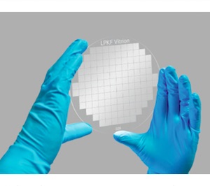
The technology company LPKF has now put a new cleanroom fab into operation to produce thin-glass components for applications in the electronics and semiconductor industry. The LIDE process (Laser Induced Deep Etching) developed by LPKF enables rapid and high-precision structuring of thin glass without impairing surface properties. The original stability of the glass remains fully intact. This process facilitates the use of glass in, for example, the production of microsystems, sensors, display components, and microchips.
The cleanroom fab was constructed in record time. Due to the considerable interest shown by the semiconductor and electronics industry in this innovative method of processing thin glass, rapid completion was required. Despite the difficult circumstances encountered this year with travel restrictions among service providers and delivery issues involving some manufacturers, the fab was constructed within a tight schedule of just 13 months. Dirk Neizel, Operations Manager at LPKF, was the driving force behind organizing and expediting the construction. “We now have a very flexible hall that we can equip in accordance with customer requirements, thus allowing the required production processes in each case to be offered as quickly as possible. With a complete air exchange every 60 seconds and precisely controllable climatic conditions, the fab optimally meets all the requirements of a production cleanroom. We have also invested heavily in modern safety technology in all systems and laboratories,” emphasizes Dirk Neizel.
Dr. Roman Ostholt heads the Electronics Business Unit, which also includes the LIDE service division under the brand name Vitrion. “We can now produce large quantities of thin-glass components and micro-components quickly and efficiently in our foundry and supply our customers worldwide,” he reports. Together with his team, he will continue to intensify and develop the cooperation with customers and partners in the semiconductor and electronics industry. In addition to the sale of its systems, this foundry constitutes a significant extension to LPKF's business model.
For CEO Dr. Götz M. Bendele, the project is indicative of LPKF's innovative strength and customer proximity: “Our new fab enables easy access to our technology for a broad set of customers across industries, who from today can order structured thin glass components from LPKF for their high-volume applications. In doing so, they can quickly realize substantial value from our transformative platform technology, without the need to invest in both systems and process capabilities. This drives our customers’ competitive advantage.”
Glass is a material of particular interest to many areas in the electronics and semiconductor sector due to its properties. For a long time, the material was considered very difficult to work with. Surface defects associated with the production process have earned glass the reputation of being prone to brittle fracture and therefore, at best, suitable for simple tasks only. Thanks to Laser Induced Deep Etching technology (LIDE), deep microstructures can now be created in glass for the first time without causing micro cracks, stresses, or other surface defects.
Processing is extremely precise, and the process is fast. Interest in using this inexpensive material is increasing at a corresponding rate. With the use of LIDE-processed glass, even better results than previously possible can now be achieved, for example, in advanced IC and wafer level packaging in heterogeneous integration. The process also opens up new opportunities for processing and using display glass or microfluidic arrays.
Share on:


Testimonial
"Your magazines are a great platform for people to exchange knowledge. Thank you for the work that you do."
Simon Khesin - Schmoll MaschinenSuggested Items
New Book Explores How UV Technology Is Transforming Electronics Protection, Efficiency, and Sustainability
05/14/2026 | I-Connect007I-Connect007 proudly announces the recent release of The Printed Circuit Designer’s Guide to…™ UV Curable Conformal Coatings, the latest installment in its highly regarded Printed Circuit Designer’s Guide to…™ book series. Authored by respected industry technologists Brian Chislea and Cody Schoener, PhD, of Dow, Inc., this new volume offers a comprehensive exploration of UV-curable conformal coatings and their expanding role in improving the protection, performance, and sustainability of electronic assemblies.
Nortech Systems Reports Q1 Results
05/14/2026 | Globe NewswireNortech Systems Incorporated, a leading provider of engineering and manufacturing solutions for complex electromedical and electromechanical products serving the medical imaging, medical device, industrial, and aerospace & defense markets, reported financial results for the first quarter ended March 31, 2026.
LITEON Technology Reports Consolidated April Sales of NT$16.7 Billion, Up 25% YoY and 1% MoM
05/14/2026 | LITEON TechnologyLITEON Technology reported its April consolidated revenue of NT$16.7 billion, up 1% M-o-M and 25% Y-o-Y. Revenue growth was mainly driven by high-end server power systems for cloud and AI applications, high‑efficiency backup battery units (BBU), and opto-electronic semiconductors.
Key Tronic Posts Results for Q3 of Fiscal Year 2026
05/14/2026 | KeytronicFor the third quarter of fiscal year 2026, Key Tronic reported total revenue of $89.6 million, compared to $112.0 million in the same period of fiscal year 2025.
New Courses: Advance Your Electronics Expertise in June and July
05/14/2026 | Global Electronics AssociationStay current with design, manufacturing, and quality standards by enrolling in one of these online instructor-led courses starting in June and July from ElectronicsU at the Global Electronics Association, designed to help professionals at every level sharpen their skills and advance their careers. These live, expert-led sessions combine flexibility with real-time interaction, allowing participants to learn directly from seasoned industry professionals while collaborating with peers worldwide. Access to all applicable IPC standards is included in the courses.