


 The Marketing Minute: If Your Marketing Budget Gets Cut in Half, Then What?
 Punching Out: How Are the Big Boys in Electronics Doing?
 It’s Only Common Sense: Complexity Is the Enemy of Profit


MKS Expands Industry Footprint in Asia with Newest HDI PCB Laser Manufacturing Solution
December 10, 2020 | MKS Instruments, Inc.Estimated reading time: 2 minutes
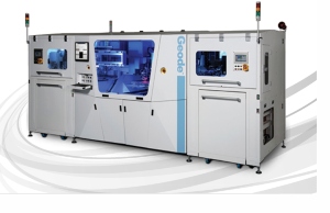
MKS Instruments, Inc., a global provider of technologies that enable advanced processes and improve productivity, announced it has received an order for multiple ESI® Geode™ HDI via drilling systems in Taiwan from a major technology leader in the HDI PCB manufacturing market.
“The market is embracing the economic advantages that the latest MKS developments have to offer,” said John Williams, Vice President and General Manager of MKS’ Equipment and Solutions division. “Our Geode HDI via drilling system meets the needs of high-volume HDI PCB manufacturing, while helping customers secure a technological advantage for current and future product requirements.”
This multi-unit order will support the customer’s existing manufacturing and future technological development through the use of leading-edge via drilling technology. Since its release to the market, the Geode HDI via drilling system has introduced HDI manufacturers to the performance advantages that ESI technology has provided to Flex PCB manufacturers for decades. The Geode platform has seen strong traction amongst the industry’s top players since its recent introduction to the market.
Developed by MKS’ Equipment & Solutions Division, already a market leader in flex PCB laser drilling solutions, the Geode system is optimized to process the rigid HDI PCBs and package substrates widely used in consumer electronics, such as smartphones and other handheld devices. Building on MKS’ technology leadership in laser processing for flexible printed circuits, Geode’s new laser technology and control capabilities deliver breakthrough performance. Its superior throughput, refined power control and small system footprint meet the needs of high-volume PCB manufacturers and technology leaders.
About MKS Instruments
MKS Instruments, Inc. is a global provider of instruments, systems, subsystems and process control solutions that measure, monitor, deliver, analyze, power and control critical parameters of advanced manufacturing processes to improve process performance and productivity for our customers. Our products are derived from our core competencies in pressure measurement and control, flow measurement and control, gas and vapor delivery, gas composition analysis, electronic control technology, reactive gas generation and delivery, power generation and delivery, vacuum technology, lasers, photonics, optics, precision motion control, vibration control and laser-based manufacturing systems solutions. We also provide services relating to the maintenance and repair of our products, installation services and training. Our primary served markets include semiconductor, industrial technologies, life and health sciences, research and defense. Additional information can be found at www.mksinst.com.
About the ESI Brand
ESI® is a brand within the MKS Instruments Equipment & Solutions Division. The ESI portfolio consists of laser-based micro manufacturing systems and component test systems that are used worldwide by manufacturers in the electronics industry to process the materials and components that are an integral part of the electronic devices and systems in use today. Leveraging over 40 years of laser-material interaction expertise and applied laser technology, ESI solutions enable customers to optimize production by providing more control, greater application flexibility and more precise processing of a wide range of materials. The result is higher production quality, increased throughput and higher back-end yields at a lower total cost-of-ownership. Additional information can be found at www.esi.com.
Share on:


Testimonial
"In a year when every marketing dollar mattered, I chose to keep I-Connect007 in our 2025 plan. Their commitment to high-quality, insightful content aligns with Koh Young’s values and helps readers navigate a changing industry. "
Brent Fischthal - Koh YoungSuggested Items
Nortech Systems Reports Q1 Results
05/14/2026 | Globe NewswireNortech Systems Incorporated, a leading provider of engineering and manufacturing solutions for complex electromedical and electromechanical products serving the medical imaging, medical device, industrial, and aerospace & defense markets, reported financial results for the first quarter ended March 31, 2026.
Top Business Groups Urge Congress to Extend, Expand Successful Semiconductor Tax Credit
05/14/2026 | SIAThe Semiconductor Industry Association (SIA) and a broad coalition of 17 other top business and trade groups in a letter urged Congress to extend the Advanced Manufacturing Investment Credit (AMIC) – a highly impactful tax credit for chip production that is set to expire at the end of this year – and expand it to cover semiconductor design and other critical R&D activities.
ONERugged Accelerates Smart Manufacturing with Rugged Computing Solutions
05/14/2026 | BUSINESS WIREAs global manufacturing continues its rapid digital transformation, enterprises are facing increasing pressure to improve production efficiency, strengthen quality control, and enable real-time operational visibility.
Absolute EMS Expands Support for LEO, MEO, and GEO Satellite Programs
05/13/2026 | Absolute EMS, Inc.Absolute EMS, Inc., a Silicon Valley–based provider of high-technology electronics manufacturing services, continues to grow its presence in the satellite sector, supporting programs across low Earth orbit (LEO), medium Earth orbit (MEO), and geostationary orbit (GEO) with advanced PCBA manufacturing, test, and sub-assembly capabilities.
New Courses: Advance Your Electronics Expertise in June and July
05/14/2026 | Global Electronics AssociationStay current with design, manufacturing, and quality standards by enrolling in one of these online instructor-led courses starting in June and July from ElectronicsU at the Global Electronics Association, designed to help professionals at every level sharpen their skills and advance their careers. These live, expert-led sessions combine flexibility with real-time interaction, allowing participants to learn directly from seasoned industry professionals while collaborating with peers worldwide. Access to all applicable IPC standards is included in the courses.