


 Standard of Excellence: The Future of Fabrication—From Art to Automation
 Knocking Down the Bone Pile: The Business Case for Component Reclamation
 Global Sourcing Spotlight: The Hidden Power of the Rep Network


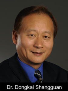
Indium Corporation’s innovative materials for advanced semiconductor packaging will be the focus of a presentation by Dr. Dongkai Shangguan, strategic advisor, at the Surface Mount Technology Association’s Wafer-Level Packaging Symposium, Feb. 15-17, San Jose, Calif., U.S.
As advanced packaging continues to drive towards heterogeneous integration, new materials need to be developed to address the many challenges faced in the assembly process. In his presentation Innovative Materials for Advanced Semiconductor Packaging, Dr. Shangguan will cover cutting-edge materials for this technology, including novel flux formulations and adhesive agents for wafer/die bonding, interactions between the flux material and various dielectric materials on the wafer, and materials for thermal management in high density packaging. The presentation will introduce the different processes and the associated materials, and the benefits and disadvantages of the various options will be discussed in detail. Proper selection and application of interconnect materials for the various assembly processes is crucial to ensuring a high production yield during the assembly process for reliable wafer-level packages.
Dr. Shangguan is a strategic advisor to Indium Corporation. In this role, he works on specific trends related to the advanced semiconductor packaging and SMT industries, and applies his significant industry experience to supporting customers. Dr. Shangguan is an IEEE Fellow and IMAPS Fellow, and has served on the boards of directors for several professional organizations and industry associations, including IPC, IEEE EPS, and iNEMI. He also serves as a Distinguished Lecturer for IEEE EPS. He has been honored with some of the industry’s most prestigious awards, including IPC’s President’s Award, the Society of Manufacturing Engineers’ (SME) Total Excellence in Electronics Manufacturing Award, the Outstanding Sustained Technical Contribution Award from IEEE EPS, and the William D. Ashman Achievement Award from IMAPS, among others. Dr. Shangguan received a B.S. in mechanical engineering from Tsinghua University, China, an MBA from San Jose State University, Calif., and a Ph.D. in materials from the University of Oxford, U.K. He has held postdoctoral positions at the University of Cambridge, U.K. and The University of Alabama, and has served as a guest professor at several universities. Dr. Shangguan has published two books and more than 200 scientific papers and technical articles, and has given numerous presentations to share knowledge and expertise with the industry. He is the inventor/co-inventor of 25 U.S. patents and several foreign patents.
Download The Printed Circuit Assembler’s Guide to… Solder Defects by Dr. Ronald C. Lasky. You can also view other titles in our full I-007e Book library here.


