


 The Right Approach: Get Ready for ISO 9001 Version 6
 Dan’s Biz Bookshelf: ‘Still Broke: Walmart’s Remarkable Transformation'
 Driving Innovation: Depth Routing Processes—Achieving Unparalleled Precision in Complex PCBs


Atotech Sells 1,000th Horizontal Electrolytic Copper Plater
June 8, 2022 | AtotechEstimated reading time: 2 minutes
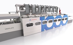
Atotech, a market leader in advanced electroplating solutions, announced the sale of its 1,000th horizontal equipment for electrolytic copper plating. The plater, which belongs to the company’s Uniplate product family, will be installed at one of Taiwan’s leading advanced package-substrate and PCB manufacturers. Atotech’s Uniplate Cu18 plating line is designed for high aspect-ratio through-hole filling of core layers for advanced packaging of CPU and MPU for high-performance processing and computing.
“The 1000th horizontal electrolytic copper plater is intended to support our customer in Taiwan in complying with the increasing demand for more advanced IC substrate products,” said Harald Ahnert, President of Atotech’s Electronics segment. “For over three decades, we have worked with leading PCB and Package Substrate companies and have shaped the industry with our innovative, constantly improved Uniplate family. This is just another step in our continued success story, and we are all proud of the innovative capacity of our global engineering teams.”
Key milestones of Atotech’s horizontal electrolytic copper plater include:
- 1988: Atotech sells its first Uniplate plater (DC plater with soluble anodes), revolutionizing the way PCBs are transported and processed by introducing horizontal electrolytic copper plating.
- 1998: Atotech launches the next-level breakthrough with a system that has an inert anode and reverse pulse plating capabilities and uses a redox system for copper replenishment.
- 2002: Atotech’s engineering teams further enhance the company’s flagship horizontal production system and launch “Uniplate InPulse 2”, the next-generation copper plater. It features closer proximity between anodes and PCB, allowing improved surface distribution and requiring no shielding system.
- Over the years, the plater series is further optimized, and more innovations are added to the product family, incl. an extra-wide plater and an advanced plater for through-hole filling.
- Atotech’s latest generation of the Uniplate plating system is used for high aspect-ratio through-hole filling of core layers for advanced package substrates. It is also used for mSAP technology as applied in the production of substrate-like PCBs, particularly flash copper plating and any-layer technology with BMV SuperFilling.
- Atotech is currently developing a new generation of its plater family with an expected market launch next year. Key features of this product will include its ability to transport much thinner materials, plate finer features, and it will come with an even more advanced surface-distribution concept for horizontal electrolytic copper plating.
- To date, Atotech has sold a total of more than 2,220 units across all its Electronics equipment systems.
The sale of the 1,000th horizontal electrolytic copper plater complements Atotech’s horizontal lines from the ‘Uniplate’ family, which are already in operation at several flagship manufacturers worldwide. The order is in line with the current trend to ramp up production capacities for high-performance computing and advanced-packaging applications.
“We believe package substrates is currently one of the most dynamic and fastest-growing segments of the printed-circuit-board markets,” said Mr. Ahnert. “Work from home, virtual conferencing, and remote learning have accelerated the digital transformation over the past two years. The rising demand for cloud computing, laptop, and servers induced the growth of the semiconductor packaging industry. This has been supported by the higher silicon content required for certain products such as computers, 5G smartphones, server/data storage, and EV/hybrid cars.
“We are very excited to work with the top global manufacturers in this area,” continued Mr. Ahnert. “Our leading R&D capabilities allow us to provide our customers with the most advanced and comprehensive solutions, helping them build next-generation package substrates for future electronics systems.“
Share on:


Testimonial
"Our marketing partnership with I-Connect007 is already delivering. Just a day after our press release went live, we received a direct inquiry about our updated products!"
Rachael Temple - AlltematedSuggested Items
New Podcast Episode Drop: MKS’ Atotech’s Role in Optimize the Interconnect
09/08/2025 | I-Connect007In this episode of On the Line With…, host Nolan Johnson sits down with Patrick Brooks, MKS' Atotech's Global Product Director, EL Systems, to discuss the critical role that wet processes play alongside laser systems in advancing the Optimize the InterconnectSM initiative. Brooks points to Bondfilm as a key example—a specialized coating that enables CO₂ lasers to ablate more effectively than ever before.
Partnerships Drive Innovation for a Brighter Manufacturing Future
08/26/2025 | Barry Matties, I-Connect007When Schweitzer Engineering Laboratories (SEL) opened its greenfield facility in 2023, it did so with careful attention to choosing its suppliers. In this discussion, Collin Peters, electronics business director for North America at MKS’ Atotech, and Justin Kennedy, manager of engineering at SEL, explore their unique partnership that includes collaborative efforts to develop innovative solutions like the Uniplate® PLBCu6 line.
New Episode Drop: MKS’ ESI’s Role in Optimize the Interconnect
08/26/2025 | I-Connect007In this latest episode, Casey Kruger, director of product marketing at MKS’ ESI, joins On the Line With… host Nolan Johnson to share how CO₂ laser technology delivers faster, more accurate vias in a smaller, more energy-efficient footprint.
SEL: Revolutionizing PCB Production Through MES, Partnerships, and Vision
08/21/2025 | Barry Matties, I-Connect007Two years ago, we visited Schweitzer Engineering Laboratories (SEL) to better understand its new captive greenfield PCB facility. We recently returned, this time to discuss how this bold vision has transformed the industry. Barry Matties met with John Hendrickson, engineering director, and Jessi Hall, vice president of vertical integration, to discuss the transformative capabilities of Factory Core, SEL’s custom manufacturing execution system (MES), which allows for real-time monitoring of workflow and machine performance, and has led to impressive improvements in quality and cost efficiency.
MKS’ Atotech to Participate in IPCA Electronics Expo 2025
08/11/2025 | AtotechMKS Inc., a global provider of enabling technologies that transform our world, announced that its strategic brands ESI® (laser systems) and Atotech® (process chemicals, equipment, software, and services) will showcase their latest range of leading manufacturing solutions for printed circuit board (PCB) and package substrate manufacturing at the upcoming 17th IPCA Show to be held at Pragati Maidan, New Delhi from August 21-23, 2025.