-

- News
- Books
Featured Books
- design007 Magazine
Latest Issues
Current Issue
Advanced Packaging and Stackup Design
This month, our expert contributors discuss the impact of advanced packaging on stackup design—from SI and DFM challenges through the variety of material tradeoffs that designers must contend with in HDI and UHDI.

Rules of Thumb
This month, we delve into rules of thumb—which ones work, which ones should be avoided. Rules of thumb are everywhere, but there may be hundreds of rules of thumb for PCB design. How do we separate the wheat from the chaff, so to speak?

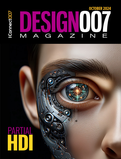
Partial HDI
Our expert contributors provide a complete, detailed view of partial HDI this month. Most experienced PCB designers can start using this approach right away, but you need to know these tips, tricks and techniques first.
- Articles
- Columns
Search Console
- Links
- Media kit
||| MENU - design007 Magazine
Torenko & Associates Offers the New 3D SPECTASCOPE from WPI Vision
August 3, 2022 | Torenko & AssociatesEstimated reading time: 1 minute
WPI Vision, a division of World Precision Instruments, is pleased to announce the appointment of Torenko & Associates at its newest manufacturers’ representative. Under the agreement, Torenko & Associates will represent the new 3D SpectaSCOPE™ inspection microscope systems throughout Mexico.
Over its 45 years in business Torenko has established strong relationships with its accounts and developed a reputation for being a leader in technology in the area. Torenko is headquartered in the Dallas/Fort Worth metroplex with other locations in the regional USA and Mexico. The company’s mission is straight-forward; Torenko & Associates strives to provide the best semiconductor, SMT manufacturing, test and repair solutions and service available. To accomplish this, the team works with some of the most innovative and reliable companies from around the globe, including WPI.
Torenko & Associates now offers the game changing 3D SpectaSCOPE, with patent-pending technology and intuitive copyrighted software. For the first time, the microscope has increased return on investment (ROI) by solving some of the problems in the PCBA process. With patent-pending technology and intuitive copyrighted software, the 3D SpectaSCOPE inspection microscope utilizes enhanced reality screen technology with high resolution cameras.
The ergonomic 3D inspection microscope features an incredible working distance of 300 mm, automatic self-focusing, integrated image capture and true 3-dimensional viewing. The 3D SpectaSCOPE lets users increase throughput while achieving greater accuracy at the highest detail. The 3D SpectaSCOPE is optimal for rework, through-hole assembly and inspections, and it is available in multiple configurations.
Suggested Items
Trane Technologies Completes Acquisition of BrainBox AI
01/03/2025 | BUSINESS WIRETrane Technologies, a global climate innovator, announced that it has completed the acquisition of BrainBox AI, a pioneer in autonomous HVAC controls and generative Artificial Intelligence (AI) building technology. The acquisition was previously announced in a press release on December 18, 2024.
Analysts: 54 Trends That Will Shape the Technology Market
01/03/2025 | ABI ResearchAs 2025 kicks off, predictions abound on the technology innovations expected in the year ahead. In its new whitepaper, 101 Technology Trends That Will—and Won’t—Shape 2025, analysts from global technology intelligence firm ABI Research.
Vortex Companies Acquires Trenchless and UV Equipment Innovator ETECAS UG
01/03/2025 | PRNewswireThe Vortex Companies, LLC (Vortex) announced the acquisition of ETECAS UG (ETECAS), a Germany-based leader in trenchless rehabilitation and UV curing equipment. Headquartered in Dietmannsried, Germany, ETECAS specializes in the development and manufacturing of cutting-edge equipment and UV curing systems for the trenchless pipeline rehabilitation industry.
TRI to Host Test and Inspection Technology Seminars
01/02/2025 | TRITest Research, Inc. (TRI) is proud to announce the 2025 Technology Seminars, which will feature Innovative Inspection Solutions, SPI, AOI, AXI, and ICT solutions at a series of technology seminars and product demos held in Taiwan, Shenzhen, and Suzhou.
ONDA Sets up Joint Venture in UAE to Speed up Expansion into the Middle East
01/01/2025 | BUSINESS WIREONDA, a South Korean AI and big data-driven hospitality technology company, has announced its plan to establish a joint venture with a UAE-based Seed Group. Leveraging Seed Group’s extensive regional networks, ONDA is accelerating its efforts to make a foray into the Middle East.


