


 Powering the Future: When Material Choice Defines RF Performance
 Learning with Leo: The Cost of Cleaning and Protecting the Ozone Layer
 Nolan’s Notes: Cleaning With Smaller Geometries


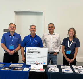
Saki Corporation, an innovator in the field of automated optical and X-ray inspection equipment, is preparing to exhibit at NEPCON Vietnam 2022. From 14 to 16 September, visitors to the Saki booth #H01 will be invited to discover the latest 3D AOI, SPI and AXI inspection solutions alongside its 2D AOI benchtop model BF-Sirius. Together with our partner JS TECH, the Saki technology team will also present latest hard- and software innovations and demonstrate its Full SMT Line, Smart Factory and M2M capabilities.
Visitors to the Saki booth #H01 will be invited to take a first-hand look at the unique features of the latest hardware and software releases with an emphasis on accuracy, speed, reliability and full-line connectivity capability for applications across all sectors.
The show line-up on booth #H01 will feature:
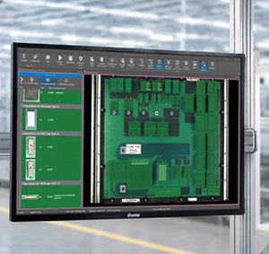
3D-AOI
3D-AOI solution: 3Di-LS2 with 12?m high resolution Z-axis optical head control feature
The 3D AOI model 3Di-LS2 with 12?m camera head is designed to improve production, boost process efficiency, and maximize product quality. Equipped with Saki’s new Z-axis optical-head control feature, the machine’s advanced capabilities for accurate inspection of tall components, press-fit components and PCBAs in jigs will be a key highlight of the show. The innovative optical-head and side camera offers the industry’s highest level of inspection capability with a height-measurement range in 3D mode up to 40mm. The focus height in 2D is also increased to 40mm. With these capabilities, Saki’s 3Di-AOI Series fulfills inspection capabilities and flexibility far beyond standard SMT inspection processes with accuracy, speed, and ease.
3D-SPI
3Si-LD2 with 12?m camera head
Saki’s high-precision and high-speed 3D solder paste inspection machine is a dual-lane system equipped with a 12µm camera head for board sizes from 50mm x 60mm to 500mm x 510mm.
2D-AOI
BF-Sirius – Benchtop Solution for Large size PCB’s
BF-Sirius is a high-speed 2D AOI benchtop model that supports large size PCBs up to 500 x 460 mm (19.7? x 18.1?). The small footprint minimizes cost and floorspace requirements. The system can inspect multiple SMT processes including selective solder and conformal coating.
AXI
Visitors to the booth will also be offered an insight into Saki’s automated X-ray inspection systems that deploy unique Planar CT technology to provide high-speed and high-accuracy solutions for ‘Real 3D’ volumetric inspection. The systems clearly identify voids in the solder of BGAs mounted on boards and non-wetting shapes such as Head-In-Pillow caused by non-wetting of solder, as well as detecting defective parts.
“As one of the world’s top exporting countries of electronics, Vietnam is a key strategic region of focus for Saki,” said Eddie Ichiyama, Saki Chief Sales Manager Overseas. “We’re incredibly excited to be exhibiting again at NEPCON Vietnam after Covid 19 restrictions have finally lifted. We can’t wait to share our expertise and knowledge with the many visitors to the show.”


