


 Elementary, Mr. Watson: PCB Education in the Midst of the Storms
 Beyond Design: How Signals Survive the Hostile PCB Environment
 Connect the Dots: What Designers Should Know About Non-conductive Via Fill


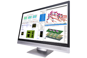
Keysight Technologies, Inc., a leading technology company that delivers advanced design and validation solutions to help accelerate innovation to connect and secure the world, announced PathWave Advanced Design System (ADS) 2023 for high-speed digital (HSD) design with new Memory Designer capabilities for modeling and simulation of next-generation interface standards such as Double Data Rate 5 (DDR5).
As data center throughput climbs, performance expectations of servers and high-performance computing drive the need for new high-density, ultra-fast memory or DDR5 Dynamic Random Access Memory (DRAM). Operating at twice the data rate of DDR4 memory results in shrinking design margins and makes it difficult for hardware designers to optimize printed circuit boards (PCB) to minimize the effects of reflection, crosstalk and jitter. In addition, lower voltages, higher currents and new requirements for equalization within the DRAM receiver create signal integrity challenges that are difficult and costly to troubleshoot.
Keysight’s PathWave ADS 2023 for HSD ensures rapid simulation setup and advanced measurements while providing designers critical insights to overcome signal integrity challenges. Its new Memory Designer quickly constructs parameterized memory buses using the new pre-layout builder, allowing designers to explore system trade-offs that reduce design time and de-risk product development for DDR5, Low-Power Double Data Rate (LPDDR5 / 5x), and Graphics Double Data Rate (GDDR6 / 7) memory systems.
“The biggest takeaway from our first DDR5 design is just how many aspects there are to consider with simulation,” said Lorenzo Forni, PCB design and SI/PI leader at SECO, an Italian industrial group that designs and produces embedded systems and IoT solutions. “You must combine the stack-up analysis, routing geometry and the AMI models. Fortunately, we used Keysight’s Memory Designer for the DDR5 simulation and it's very automated. The configurations are built-in and it's very easy. The setup of the Memory Designer schematic reduced the amount of time needed, and simulation caught many issues during our design process.”
“Keysight has a long history of being on the forefront of channel simulation technology as well as test leadership in memory industry standards bodies including JEDEC,” said Stephen Slater, director of PathWave HSD product management at Keysight Technologies. “We are committed to building the widest portfolio of products and services for DDR enablement, including a complete design-to-test workflow for DDR5 memory from simulation to probing and fixturing. As a result, our HSD design customers experience a more predictive flow and higher confidence at design signoff.”
Keysight’s PathWave ADS 2023 key customer benefits include:
Accurate Simulation and Modeling
- Supports a broad range of next-generation standards: LPDDR4, LPDDR5, GDDR6, GDDR7, HBM2/2E, HBM3, and NAND
- Accurately predicts the closure and equalization of the Data Eye: minimizes impact of jitter, ISI and crosstalk using single-ended I/O (Input-Output) buffer information specification algorithmic modeling interface (IBIS-AMI) modeling with forwarded clocking, DDR bus simulation and accurate electromagnetic (EM) extraction of PCB signal routing
- Shortens time-to-market with a single design environment that enables pathfinding in pre-silicon digital twins to address current integration requirements such as forwarded clocking and timing, IBIS algorithmic modeling interface (IBIS-AMI) modeling and compliance tests and future challenges like single-ended Pulse Amplitude Modulation 4 level (PAM4), for exploration of DDR6
Rapid Simulation Times
- Rapidly generates buses via a parameterized pre-layout builder which enables designers to quickly generate wide buses of memory signals and easily create flexible schematics to explore trade-offs
- Completes simulation up to 80 percent faster: cloud-based high-performance computing (HPC) utilizes parallel processing to accelerate Memory Designer and EM simulation run times
Linking Simulation to Test
- Automates design-to-test workflows with an easy connection between simulation and measurement domains to enable comparison of the stored data against measured results from physical prototypes


