


 SMT Perspectives & Prospects: The Architecture of Winston Churchill’s Leadership
 Global Sourcing Spotlight: Making Global Sourcing Simple Again
 The Government Circuit: New Council Now Helps Shape Policy Decisions in the Electronics Supply Chain


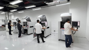
Saki Corporation, an innovator in the field of automated optical and X-ray inspection equipment, announces the opening of its new solution center – the “Saki Solution Center Thailand” – in Nonthaburi, Thailand. As well as comprising the recently relocated main offices for Saki Asia Pacific (Thailand) Co. Ltd., the modern facility houses a wide range of Saki’s inspection machines for on-site and online demonstrations and hands-on access to customers looking to gain a complete understanding of Saki’s Total Line Inspection Solution. The opening ceremony was held on November 29, 2022.
At the Saki Solution Center Thailand, Saki's total solution for smart factories will be on permanent exhibit for demonstrations and technical training. Comprising 3D solder printing automatic inspection equipment (3D-SPI), 2D automatic visual inspection equipment (2D-AOI), and the latest next-generation 3D-AOI equipment, Saki’s range incorporates advanced hardware and integrated machine-2-machine software for the smooth running of quality assurance in PCB and component manufacture. In 2023 a 3D-AXI machine will be added to the center’s lineup.
Located in the capital city of Bangkok, the Saki Solution Center Thailand can easily be accessed from both of Bangkok’s major airports, offering easy access for partners and customers to experience demonstrations, technical training, and inspection tests. A dedicated meeting room allows for in-depth discussion of customized software and hardware solutions with on-site service engineers. Customers looking to solve their manufacturing quality assurance issues are invited to book a complete interactive demonstration tailored to their specific products and exacting needs.
A facility not only for Thailand-based customers, the Saki Solution Center Thailand has been developed as a demonstration hub for manufacturers across the Asia-Pacific region and worldwide. Customers from Europe and the Americas with manufacturing facilities in the Asia-Pacific region are encouraged to schedule a visit while touring their own factories, typically only one to two hours flight away. The center is also equipped with sophisticated online demonstration facilities for customers unable to visit personally.
Machines on show include:
- 3D-SPI
- 3Si-LS2-L 18µm
- 2D-AOI
- BF-Comet18
- BF-Frontier II
- 2Di-LU1
- 3D-AOI
- 3Di-LS2-L 12µm
- NEW 3Di-LS3 8µm
- 3D-AXI – Coming 2023
- 3Xi-M110
“The ability to have a hands-on experience with Saki’s world-class machines allows for a far greater understanding of our total inspection line solution for both new and existing customers,” said Jayson Moy, General Manager Saki Asia Pacific Thailand. “We are excited to welcome partners and customers from around the world for a demonstration of the impressive speed and accuracy of our products.”
The new address for Saki Asia Pacific (Thailand) Co. Ltd. is:
89 COSMO Office Park, 1st Floor Unit 10,
Popular Road,
Tambol Banmai, Amphur Pakkred,
Nonthaburi 11120,
Thailand
Tel. +66-2-0658899
Fax. +66-2-0656665


