


 Powering the Future: When Material Choice Defines RF Performance
 Learning with Leo: The Cost of Cleaning and Protecting the Ozone Layer
 Nolan’s Notes: Cleaning With Smaller Geometries


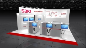
Saki Corporation, an innovator in the field of automated optical and X-ray inspection equipment, will be exhibiting its latest high-speed, premium accuracy in-line inspection solutions at the 37th NEPCON JAPAN in Tokyo, Japan. From January 25 - 27, visitors are invited to chat with the Saki team on Booth #15-1, East Hall 2, where Saki’s industry-leading inspection machines will be available for hands-on demonstrations. Booth highlights will include Saki’s 3D automated optical inspection equipment (3D-AOI) equipped with the latest optional functions and Saki’s innovative X-ray inspection solution (3D-AXI) that enables high-speed, high-precision in-line inspection for high-density mounting boards and ultra-small parts.
Saki’s booth will feature three 3D inspection machines, allowing booth visitors to experience the solutions up-close and gain an in-depth understanding of their performance directly from the Saki technical team at the show:
New 3D-AOI
3Di-LS3 and 3Di-MS3 – From Saki's new 3D-AOI 3Di series lineup, the 3Di-LS3 and 3Di-MS3 will be exhibited. The new 3Di series enables high-speed and high-performance inspection while achieving both high resolution and expanded height measurement with an upgraded high-resolution camera system. It offers a wide variety of features that can be selected according to the customer's production environment and product requirements. These optional functions enhance scalability and contribute to greater quality assurance and improved productivity. Equipped with an 8?m high-resolution camera system, the 3Di-LS3 supports assembly inspection of SMT-mounted parts, including extremely small and tall parts, with the industry's fastest cycle time. The 3Di-MS3 has a compact design suitable for medium size board inspection. It will be introduced at NEPCON JAPAN on the Saki booth together with the latest options that permit on-site upgrades.
3D-AXI
3Xi-M110 – with Saki’s optimized Planar CT software, developed in-house for incredible cycle-time improvements, this compact and lightweight 3D-AXI system provides impressive quality assurance with highly accurate void measurement and detection for both PCBs and components. It contributes to quality assurance with high-precision inspection by capturing solder joint defects and minute shape deformities in high-density circuit boards and components. Visitors to the Saki booth will personally witness the significant inspection speed enhancements the 3Xi-M110 provides, as well as being among the first to glimpse the exciting improvements of the latest M110 model.
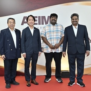
Ken Katsumi, Chief Sales Manager of Saki's Sales Headquarter, said "Saki's high-quality in-line inspection technology, which realizes advanced automatic 100% inspection, is the perfect choice for customers who seek highest reliability, including those in the automotive industry. We will introduce the latest solutions that meet the quality requirements that our clients demand. We are looking forward to your visit."


