


 Flexible Thinking: Designing Flex Circuits for Dynamic Reliability
 Global PCB Connections: Rigid-flex and Flexible PCBs—The Backbone of Modern Electronics
 Happy’s Tech Talk #29: Bend-to-Install Semi-flex FR-4


Insulectro, the largest distributor of materials for use in the manufacture of printed circuit boards and printed electronics, has opened a testing and development laboratory for Kyocera tools in its Lake Forest, California headquarters. The lab was created in association with backup and entry materials manufacturer LCOA in that company’s plant.
“I am pleased to announce that Insulectro, the exclusive North American distributor of drills, routers, endmills, and other cutting tools manufactured by Kyocera, will begin offering a variety of services from a new laboratory on our Lake Forest campus,” announced Geraldine Arseneau, Insulectro Product Manager for the Kyocera product line, “This will enable us to build on the synergy of Kyocera’s best-in-class tools and Insulectro’s dominance in drill room backup and entry products.” Arseneau joined Insulectro several years ago after a lengthy career with Kyocera.
The new lab is expected to support new product design, troubleshoot field issues, and include design feature testing, DoE (Design of Experiments) studies, confirmation testing, and repoint cycling testing.
It will determine proper feed and speed parameters for common PCB applications, develop processing parameters for new industry materials to understand how new technologies affect product performance, and supply customers with complete solutions. The Lab will also support industry and competitor benchmark studies.
Joe Negron, Kyocera Sales Manager, said, “The lab is a large next step for the Kyocera/Insulectro team. It vastly increases our capability to service our customers as technology changes.”
The Lab is equipped with a Schmoll drill/router (dual spindle drill with 160KRPM and router 50KRPM); a Microview CMM used to measure positional accuracy; and a Haas CM-1: compact CNC vertical machining center (50KRPM spindle, 5 HP motor).
It also includes a Struers automated polisher/grinder for X-sections; an Olympus Toolmakers microscope; and a metallograph to measure hole wall quality.
Insulectro Vice President of Product Management Michelle Walsh is also enthused about the additional capabilities, “This month we hosted a joint meeting of the Kyocera Team with Insulectro’s leadership and operations teams. We were all very excited not only about the Lab’s value for our existing customers but how we now have the capability to run studies to promote product offerings and qualifications requested by new customers. Fabricators can continue to count on Insulectro for the developing technological information.”
Kyocera SGS designs and manufactures tight tolerance precision carbide cutting tools for PCB applications. Products include drills, routers, end mills, and specialized cutting tools ranging from 0.05mm to 6.70mm diameters (0.0020" - 0.2638").
Kyocera’s renowned array of drills, routers, endmills, and specialty tools offer many benefits and advantages to customers for all their drilling and routing needs. Kyocera’s tool reliability and design flexibility are key strengths of their products, along with a complete R&D facility in the US, new tool manufacturing capability, and local technical resources, all available to support customer needs.
Insulectro supplies advanced engineered materials manufactured by Isola, DuPont, LCOA, CAC, Inc., Pacothane, Focus Tech, JX Nippon, TADCO, EMD Electronics (Ormet), Shikoku, Denkai America, ETI, Industrial Brush Corporation, Kyocera SGS Precision Tools, InduBond, and Shur-loc. These products are used by its customers to fabricate complex, multilayer circuit boards and to manufacture printed electronics components. Insulectro serves a broad customer base manufacturing rigid, rigid/flex, and flexible circuit boards for applications in a variety of end markets including aeronautics, telecom, data communications, high speed computing, mobile devices, military, and medical. Insulectro combines its premier product offering with local inventory across North America, fabrication capabilities and backed up by expert customer and technical support services.
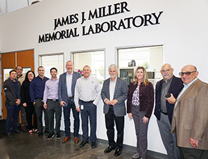
From Left to Right - Steve Komin, Senior Materials & Logistics Manager – Kyocera; Russ Reynoso, Design Engineering Manager – Kyocera; Geraldine Arseneau, Drill Product Manager – Insulectro; Curtis Vozar, Director of Material & Planning – Kyocera; Jeff Zaucha, Chief Financial Officer – Kyocera; Patrick Redfern, President & CEO – Insulectro; Dave Reiter, VP of Manufacturing – Kyocera; Tom Haag, President – Kyocera; Michelle Walsh, VP of Product Management – Insulectro; Joe Negron, Sales Manager PCB and MIT – Kyocera; Ken Parent, Chief Operating Officer – Insulectro.


