


 Designers Notebook: Layer Stackup Planning for RF Circuit Boards
 Connect the Dots: Involving Manufacturers Earlier Prevents Downstream Issues
 Global PCB Connections: The Next Wave of HDI PCBs– How Design Engineers Can Stay Ahead


Optimizing Communication Between Fabricators and Designers
March 21, 2023 | Andy Shaughnessy, Design007 MagazineEstimated reading time: 4 minutes
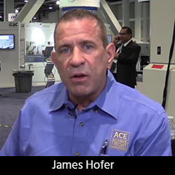
During DesignCon, I spoke with James Hofer from Accurate Circuit Engineering about some of his customers' biggest challenges. We discussed various ways to increase the level—and quality—of communication between designers and fabricators.
James also offered some interesting observations about bridging the gap between designer and fabricator. How often do you communicate with your fabricator?
Andy Shaughnessy: James, you mentioned some of the unique challenges that your customers face. Tell us about their challenges.
James Hofer: We’re doing more phased-array antennas and stacked laser-drilled microvias than ever before, but we’re still having a disconnect between the layout folks and the manufacturer, wherein they forget to stagger the vias; staggering is important. If you stack your microvias directly on top of each other, you risk intersection separation, which means when the vias heat up, they crack open at the interface between vias and the break the connection; when they cool down, they reconnect. This is caused by Z-axis expansion due to the mismatch of CTEs of the copper plating and the epoxy via fill. There are two methods of mitigating this phenomenon: copper filling the vias that are being stacked, and staggering vias slightly off center so that the stacked pad hits the pad at the via underneath it—not directly onto the hole of the via underneath. That will help with the “separation anxiety.”
I also run into designers who stack the microvias, but they’ll leave an artifact in their layout as a through-hole. If it’s not caught by them, it may also not be caught in a typical manufacturer’s DRC and we may see that as a drilled hole and not a stacked laser. If we don’t catch that, then we find ourselves trying to drill through stacked microvias, which could scrap the build. I had a rather big customer almost go through that. I spent half the day here on a conference call with them. But every customer’s task is important. I would prefer to spend a little time with them while they’re doing the layout or the designing of the boards to help them understand why we do what we do.
It’s one thing just to tell customers, “You have to do it this way.” But it’s more important for them to understand why they should do it and what problems it could cause if one decides not to. If somebody doesn’t want to listen to us, that’s fine, but discuss it with us so we can put steps in place to mitigate the issues that arise by not doing it.
Shaughnessy: Most PCB designers have been doing this at least 30 years. Why is there still a communication gap between designers and fabricators?
Hofer: There always has been a bit of a separation between the electrical engineer, the designer, and the manufacturer. Everybody feels as though they know the right way to do this, and you can get in a certain groove with subject matter experts. You might have a longtime manufacturer who knows exactly how to make your boards robust enough to work right every time, but then you switch manufacturers and they don’t know what you’re doing. They’re not used to you doing it this way or that way, so they don’t put in the steps to make sure things are as robust as possible.
Unfortunately, a lot of fabricators say, “This is the way to note it because this is the way we do it.” When we do a DFM with a customer, we suggest that they know the best way to clarify what they want and put that in a language that’s universal to all fabricators, not just one.
Shaughnessy: You’re ensuring that it’s not just tribal knowledge.
Hofer: Right, it should not be tribal knowledge. Maybe you change fabricators because I am busy, or you don’t like my price and you go away for a little while. I don’t want you telling the other fabricator, “It turns out that James only told us the way ACE does it, so I didn’t know that we needed to state our requirements that way.”
Someone just mentioned to me that a few fabricators have an online tool they can use to generate Gerbers. But I told him that they’re not really Gerbers; they’re proprietary software tools for that fabricator. I said, “If you go somewhere else, they won’t be able to use these files, and now you’re locked into that fabricator unless you pay for new Gerbers” That’s not good. I believe designers should be given as much information as possible, whether they stay with a particular manufacturer or not. I believe that we as manufacturers have a responsibility to help designers have knowledge of not only the particular manufacturers nuances but also if industry standards, so they might carry that knowledge with them no matter where they have there project built.
Shaughnessy: Either way, they’ll still remember that you tried to help them and not just nickel and dime them to death.
Hofer: That’s right. One more thing, and I don’t know if it’s a good or a bad habit, but we ask a million questions, always clarifying what we’re doing. This goes back to what I said at the beginning: “Don’t just understand what we do, but why we do it.” Then they can decide, “You know what? We’re not worried about that.” Give them the information so they can decide for themselves. If they go to another fabricator, they might find that fabricator doesn’t work like we do.
Shaughnessy: Well, that’s good stuff. Any closing thoughts?
Hofer: I’m glad to be here at DesignCon. I’m glad to see everyone getting back on the road again.
Shaughnessy: Great talking to you, James.
Hofer: Thanks for coming by.
Share on:


Suggested Items
Elephantech: For a Greener Tomorrow
04/16/2025 | Marcy LaRont, PCB007 MagazineNobuhiko Okamoto is the global sales and marketing manager for Elephantech Inc., a Japanese startup with a vision to make electronics more sustainable. The company is developing a metal inkjet technology that can print directly on the substrate and then give it a copper thickness by plating. In this interview, he discusses this novel technology's environmental advantages, as well as its potential benefits for the PCB manufacturing and semiconductor packaging segments.
Trouble in Your Tank: Organic Addition Agents in Electrolytic Copper Plating
04/15/2025 | Michael Carano -- Column: Trouble in Your TankThere are numerous factors at play in the science of electroplating or, as most often called, electrolytic plating. One critical element is the use of organic addition agents and their role in copper plating. The function and use of these chemical compounds will be explored in more detail.
IDTechEx Highlights Recyclable Materials for PCBs
04/10/2025 | IDTechExConventional printed circuit board (PCB) manufacturing is wasteful, harmful to the environment and energy intensive. This can be mitigated by the implementation of new recyclable materials and technologies, which have the potential to revolutionize electronics manufacturing.
Connect the Dots: Stop Killing Your Yield—The Hidden Cost of Design Oversights
04/03/2025 | Matt Stevenson -- Column: Connect the DotsI’ve been in this industry long enough to recognize red flags in PCB designs. When designers send over PCBs that look great on the computer screen but have hidden flaws, it can lead to manufacturing problems. I have seen this happen too often: manufacturing delays, yield losses, and designers asking, “Why didn’t anyone tell me sooner?” Here’s the thing: Minor design improvements can greatly impact manufacturing yield, and design oversights can lead to expensive bottlenecks. Here’s how to find the hidden flaws in a design and avoid disaster.
Real Time with... IPC APEX EXPO 2025: Tariffs and Supply Chains in U.S. Electronics Manufacturing
04/01/2025 | Real Time with...IPC APEX EXPOChris Mitchell, VP of Global Government Relations for IPC, discusses IPC's concerns about tariffs on copper and their impact on U.S. electronics manufacturing. He emphasizes the complexity of supply chains and the need for policymakers to understand their effects.