


 It’s Only Common Sense: Stay Curious, My Friends
 The Marketing Minute: AI Is Watching Your Marketing Habits


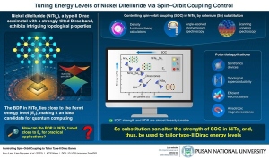
Type-II Dirac semimetals are quantum materials with unique energy level structures, such as a bulk Dirac point (BDP). However, these semimetals are unsuitable for real-life applications because their BDP is far off the "Fermi energy level." Nickel ditelluride (NiTe2), a newly reported type-II Dirac semimetal has a BDP slightly above the Fermi level. Now, researchers have substituted tellurium with selenium in NiTe2 to alter the strength of its spin-orbit coupling and further tune its BDP.
Quantum materials, such as topological semimetals, are materials whose electronic properties are linked to exotic quantum effects. While their interior is a semimetal (e metal with properties between a conductor and semiconductor), the surface behaves like a conductor. This unique electronic behavior arises due to the topology (special geometric properties) of the energy levels occupied by the electrons on the surface of these materials. Specifically, the energy levels closest to the Fermi level (EF)—the highest energy level that an electron can occupy at 0K—form up and down Dirac cones whose tips touch at Dirac points.
Materials with tilted Dirac cones are known as type-II Dirac topological semimetals and have potential applications in topological quantum computing. However, there is a bottleneck. Quantum computers need type-II Dirac semimetals whose bulk Dirac point (BDP) is close to the EF—a rarity. Scientists recently reported that nickel ditelluride (NiTe2) has a BDP slightly above the EF, making it an ideal candidate for quantum computing.
Recently, a research team, led by Associate Professor Jaekwang Lee of Pusan National University, developed a novel technique for further tuning the BDP around the EF in NiTe2. Their work was made available online on 15 July 2022 and published in Volume 16, Issue 7 of the ACS Nano journal on 26 July 2022.
Using density functional theory calculations, the researchers show that substituting tellurium (Te) with selenium (Se) reduces the strength of the spin-orbit coupling (SOC)—the interaction between the electron's spin and its orbital motion around the atomic nucleus—in NiTe2. This shifts the BDP while preserving the type-II Dirac band.
"DFT calculations shows that the SOC strength and the BDP are almost linearly tunable. Scanning tunneling microscopy and angle-resolved photoemission spectroscopy confirm that the BDP in the NiTe2?xSex alloy moves from +0.1 eV (NiTe2) to ?0.3 eV (NiTeSe) about the EF. Further, the BDP is at the exact EF for NiTe1.4Se0.6," highlights Prof. Lee.
Hence, NiTe2?xSex alloys offer a versatile platform for facilitating numerous technologies based on topological effects, including next-generation electronics, spintronics devices, efficient electrocatalysis, topological superconductivity, and quantum computers.
In conclusion, Prof. Lee discusses the longer-term implications of this work. "It provides insights into SOC control to tailor type-II Dirac bands, and will open up new avenues for exploring and developing materials with unconventional electronic properties."


