-

-
News
News Highlights
- Books
Featured Books
- smt007 Magazine
Latest Issues
Current Issue
Spotlight on Mexico
Mexico isn’t just part of the electronics manufacturing conversation—it’s leading it. From growing investments to cross-border collaborations, Mexico is fast becoming the center of electronics in North America. This issue includes bilingual content, with all feature articles available in both English and Spanish.

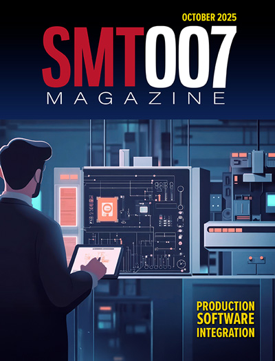
Production Software Integration
EMS companies need advanced software systems to thrive and compete. But these systems require significant effort to integrate and deploy. What is the reality, and how can we make it easier for everyone?

Spotlight on India
We invite you on a virtual tour of India’s thriving ecosystem, guided by the Global Electronics Association’s India office staff, who share their insights into the region’s growth and opportunities.
- Articles
- Columns
- Links
- Media kit
||| MENU - smt007 Magazine
Reduce Board Skyline With Solid Cavity Design
July 20, 2023 | Kris Moyer, IPCEstimated reading time: 2 minutes
With the increasing shrinkage of modern electronics in both board size and product volume, it’s becoming more difficult to mount components to the PCB surface and still meet volumetric requirements. To avoid chip-on-board (COB) processing, board cavities can help mitigate the Z-axis skyline volumetric issues and allow for components that would otherwise not fit within the skyline to be used.
As the name implies, a cavity is the removal of some of the board material to expose traces and contact pads on inner layers of the PCB. This is done to allow attachment of the component to these exposed pads rather than pads on the surface of the PCB (Figure 1). To form cavities, several special processes need to be considered. Among these are inner layer plating, particularly the effects of plating and surface finish on inner layer impedance for signal integrity; sequential lamination; surface finish on exposed inner layer pads; and the use of controlled depth milling to form the cavity, just to name a few.
Figure 1: A typical cavity as it appears in an ECAD software tool.
One of the first items of concern is the effect of plating and surface finish on impedance of the inner layers. When cavities are formed without sequential lamination, the plating and surface finish needed to support the soldering process will add conductive material thickness to the exposed areas of the inner layer. This in turn will cause an impedance discontinuity due to these different thicknesses of the traces.
Additionally, the removal of the reference planes from one side of the conductor changes the structure of the transmission line from a stripline on inner layer to a microstrip in the cavity. Most ECAD and SI tools do not support different transmission line structures on the same layer of the board. There are some solutions to this conundrum: Rather than relying on the built-in transmission line structures of ECAD tools, the designer can manually calculate the controlled impedance trace widths for the stripline and microstrip sections and then use area constraint rules to define the widths both in the cavity and on the remainder of the layer.
One possible way around this issue is to use sequential lamination to allow plating on the entire layer. But sequential lamination poses its own problems. First, it is a more costly and time-consuming process. Second, it adds fabrication allowances. It may also require the use of blind and/or buried vias to make the connections between layers. The multiple plating cycles needed for sequential lamination can cause other fabrication issues. It is recommended that the fabricator be consulted on any sequential lamination PCB design.
To read this entire article, which appeared in the July 2023 issue of Design007 Magazine, click here.
Testimonial
"Your magazines are a great platform for people to exchange knowledge. Thank you for the work that you do."
Simon Khesin - Schmoll MaschinenSuggested Items
Indium to Showcase High-Reliability Solder and Flux-Cored Wire Solutions at SMTA International
10/09/2025 | Indium CorporationAs one of the leading materials providers in the electronics industry, Indium Corporation® will feature its innovative, high-reliability solder and flux-cored wire products at SMTA International (SMTAI), to be held October 19-23 in Rosemont, Illinois.
‘Create your Connections’ – Rehm at productronica 2025 in Munich
10/08/2025 | Rehm Thermal SystemsThe electronics industry is undergoing dynamic transformation: smart production lines, sustainability, artificial intelligence, and sensor technologies dominate current discussions.
SASinno Americas Introduces the Ultra Series
10/07/2025 | SASinno AmericasSASinno Americas has introduced the new Ultra Series, the latest generation of offline selective soldering systems. Available in two models—the Ultra-i1 and Ultra-i2—the new series is designed to meet the needs of manufacturers running small to medium batch sizes, multiple product types, and frequent line changes, while maintaining exceptional precision and process control.
Elmotec by E-Tronix to Showcase SolderSmart® TOP Robotic Soldering at The Assembly Show 2025
10/06/2025 | ELMOTECE-tronix, a Stromberg Company, is pleased to announce its participation at The Assembly Show 2025 in Rosemont, IL, October 21st through 23rd. Exhibiting under Elmotec by E-Tronix, Booth #448, the team will highlight the SolderSmart® TOP robotic soldering system, featuring live demonstrations throughout the show.
SolderKing Marks Seven Years of Growth and International Recognition
10/01/2025 | SolderKing Assembly Materials Ltd,SolderKing Assembly Materials Ltd, a leading UK-based manufacturer of soldering materials and consumables, is celebrating seven years of innovation, growth, and international success.


