


 Knocking Down the Bone Pile: The Business Case for Component Reclamation
 Global Sourcing Spotlight: The Hidden Power of the Rep Network
 Smart Automation: When Traditional Depaneling Methods Reach Their Limits


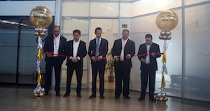
Saki Corporation, an innovator in the field of automated optical and X-ray inspection equipment, announces the opening of its new Mexican office in Zapopan, Jalisco. Perfectly situated in the manufacturing hub of the Guadalajara Metropolitan Area, the new office is the home for Saki’s subsidiary, Saki America de México S.A. de C.V. With direct links for customers across the North and South American continents, Saki’s modern facility offers an important location for service, sales, and demonstrating of its world-class range of electronics manufacturing inspection machines. The opening ceremony was held on August 8, 2023.
With its new Mexican subsidiary and dedicated facility, Saki improves further on its impressive global sales and distribution network. For customers across Mexico, as well as those in the US, Canada, and South America, the new center provides a location for demonstrations and further understanding of Saki’s Total Inspection Line Solution - a range of top-quality inspection machines with integrated software and hardware that offers unparalleled efficiency for smart factories.
Saki’s portfolio of quality assurance equipment includes 3D solder printing automatic inspection (3D-SPI), 2D automatic visual inspection (2D-AOI), the latest next-generation 3D-AOI, and cutting-edge 3D-AXI machinery for superior x-ray inspection of PCBs and components. Saki hardware and software is developed in tandem for seamless M2M integration with both sister equipment and third-party production line machines.
With an office in the Guadalajara Metropolitan Area, Saki has carefully selected a location to provide local service to one of the greatest electronic manufacturing regions in the Americas. Both established customers in the area and those who are considering Saki’s equipment for the first time will benefit from local support and the ability to discuss Saki’s range with experienced specialist engineers and sales advisors. Plans for the office include demonstrations and technical training with some of the most knowledgeable Saki engineers in the world.
Customers can visit Saki’s new office in Zapopan to better understand how to solve their manufacturing quality assurance issues and develop future-looking smart factories with lower maintenance overheads, reducing staffing costs and superior product delivery.
“Opening an office in the key region of Guadalajara shows how Saki both values and provides for its international customers,” said Norihiro Koike, President and CEO of Saki Corporation. “Saki products represent the pinnacle of electronics quality assurance, and we are excited to serve the Americas from this important central location.”
Ricardo Fuentes, Sales Manager at Saki’s regional distribution partner PAC Mexico S.A. de C.V. added: “We are delighted to have strong backing from Saki with its new office in Mexico, in order to boost sales of Saki equipment in the Mexico region and strengthen technical support for our customers.”


