-

- News
- Books
Featured Books
- design007 Magazine
Latest Issues
Current Issue
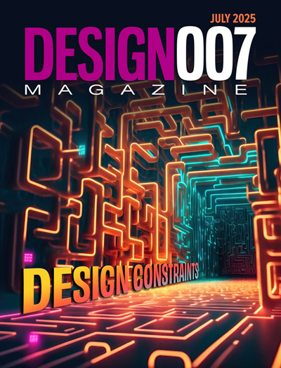
Showing Some Constraint
A strong design constraint strategy carefully balances a wide range of electrical and manufacturing trade-offs. This month, we explore the key requirements, common challenges, and best practices behind building an effective constraint strategy.

All About That Route
Most designers favor manual routing, but today's interactive autorouters may be changing designers' minds by allowing users more direct control. In this issue, our expert contributors discuss a variety of manual and autorouting strategies.

Creating the Ideal Data Package
Why is it so difficult to create the ideal data package? Many of these simple errors can be alleviated by paying attention to detail—and knowing what issues to look out for. So, this month, our experts weigh in on the best practices for creating the ideal design data package for your design.
- Articles
- Columns
- Links
- Media kit
||| MENU - design007 Magazine
Three Ways to Improve High-Speed PCB Signoff, Part 1
September 6, 2023 | Brad Griffin, Cadence Design SystemsEstimated reading time: 1 minute
Signal integrity (SI) and power integrity (PI) are top priorities for engineers designing today’s high-speed, high-density circuit boards, and faster signoff of designs can be achieved by uncovering SI/PI issues early in the design process, before costly respins are required. Three key issues engineers need to overcome to sign off on high-speed PCB designs include power analysis, serializer/deserializer (SerDes) link compliance, and double data rate (DDR) memory interface compliance.
The power delivery network (PDN) must be sufficient, efficient, and stable, and the signal quality must meet memory interface and serial link compliance specifications. This article highlights a PCB design methodology that empowers PCB design teams to create successful products on time and on budget without waiting for SI and PI specialists who may not be readily available.
Design Analysis Frameworks
There are several important frameworks to consider when designing PCBs (Figure 1).
Figure 1: Design analysis frameworks.
The design begins with the schematics, followed by the layout, and then, late in the layout phase, a detailed analysis is done to ensure the layout functions properly. During the design cycle tasks, priorities and focus change, but one critical rule of thumb is that the earlier problems are uncovered and corrected, the better.
Electronic product development has traditionally embraced a workflow in which the detailed simulation, analysis, and optimization takes place at a very late stage in the design process, often as the final step of verification and signoff. However, this delay inevitably leads to costly issues that derail budgets and delay time to market. Defects in requirements and performance are uncovered that require additional cycles to address these issues, which could have been discovered and mitigated earlier in the design phase.
To read this entire article, which appeared in the August 2023 issue of Design007 Magazine, click here.
Testimonial
"Advertising in PCB007 Magazine has been a great way to showcase our bare board testers to the right audience. The I-Connect007 team makes the process smooth and professional. We’re proud to be featured in such a trusted publication."
Klaus Koziol - atgSuggested Items
Setting Design Constraints Effectively
07/31/2025 | Stephen V. Chavez, Siemens EDAPCB design requires controlling energy within the medium of a PCB. The manner in which we control the chaos of energy is by implementing and utilizing physical and electrical rules, known as constraints, along with a specific structure and material(s) that make up what is known as the foundation of the design. These rules govern everything within the PCB structure and generally fall into two camps: performance and manufacturability. Setting this foundation correctly is extremely important and the key to success.
MacDermid Alpha Electronics Solutions Unveils Unified Global Website to Deepen Customer, Talent, and Stakeholder Engagement
07/31/2025 | MacDermid Alpha Electronics SolutionsMacDermid Alpha Electronics Solutions, the electronics business of Elements Solutions Inc, today launched macdermidalpha.com - a unified global website built to deepen digital engagement. The launch marks a significant milestone in the business’ ongoing commitment to delivering more meaningful, interactive, and impactful experiences for its customers, talent, and stakeholders worldwide.
Ansys 2025 R2 Enables Next-Level Productivity by Leveraging AI, Smart Automation, and Broader On-Demand Capabilities
07/30/2025 | PRNewswireAnsys, now part of Synopsys, announced 2025 R2, featuring new AI-powered capabilities across the portfolio that accelerate simulation and expand accessibility.
Connect the Dots: Sequential Lamination in HDI PCB Manufacturing
07/31/2025 | Matt Stevenson -- Column: Connect the DotsAs HDI technology becomes mainstream in high-speed and miniaturized electronics, understanding the PCB manufacturing process can help PCB design engineers create successful, cost-effective designs using advanced technologies. Designs that incorporate blind and buried vias, boards with space constraints, sensitive signal integrity requirements, or internal heat dissipation concerns are often candidates for HDI technology and usually require sequential lamination to satisfy the requirements.
Target Condition: The 5 Ws of PCB Design Constraints
07/29/2025 | Kelly Dack -- Column: Target ConditionHave you ever sat down to define PCB design constraints and found yourself staring at a settings window with more checkboxes than a tax form? You’re not alone. For many designers—especially those newer to the layout world—the task of setting up design constraints can feel like trying to write a novel in a language you just started learning.


