


 Standard of Excellence: Speed vs. Quality in Customer Service
 Knocking Down the Bone Pile: Revamp Your Components with BGA Reballing
 Global Sourcing Spotlight: Balancing Speed and Flexibility Without Sacrificing Control


Intel Unveils Industry-Leading Glass Substrates to Meet Demand for More Powerful Compute
September 18, 2023 | IntelEstimated reading time: 3 minutes
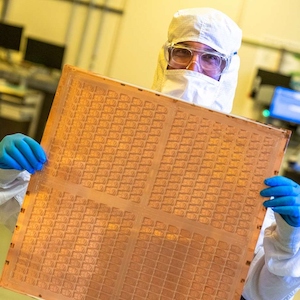
Intel announced one of the industry’s first glass substrates for next-generation advanced packaging, planned for the latter part of this decade. This breakthrough achievement will enable the continued scaling of transistors in a package and advance Moore’s Law to deliver data-centric applications.
“After a decade of research, Intel has achieved industry-leading glass substrates for advanced packaging. We look forward to delivering these cutting-edge technologies that will benefit our key players and foundry customers for decades to come,” said Babak Sabi, Intel senior vice president and general manager of Assembly and Test Development.
Compared to today’s organic substrates, glass offers distinctive properties such as ultra-low flatness and better thermal and mechanical stability, resulting in much higher interconnect density in a substrate. These benefits will allow chip architects to create high-density, high-performance chip packages for data-intensive workloads such as artificial intelligence (AI). Intel is on track to deliver complete glass substrate solutions to the market in the second half of this decade, allowing the industry to continue advancing Moore’s Law beyond 2030.
By the end of the decade, the semiconductor industry will likely reach its limits on being able to scale transistors on a silicon package using organic materials, which use more power and include limitations like shrinkage and warping. Scaling is crucial to the progress and evolution of the semiconductor industry, and glass substrates are a viable and essential next step for the next generation of semiconductors.
As the demand for more powerful computing increases and the semiconductor industry moves into the heterogeneous era that uses multiple “chiplets” in a package, improvements in signaling speed, power delivery, design rules and stability of package substrates will be essential. Glass substrates possess superior mechanical, physical and optical properties that allow for more transistors to be connected in a package, providing better scaling and enabling assembly of larger chiplet complexes (called “system-in-package”) compared to organic substrates in use today. Chip architects will have the ability to pack more tiles – also called chiplets – in a smaller footprint on one package, while achieving performance and density gains with greater flexibility and lower overall cost and power usage.
Glass substrates will initially be introduced into the market where they can be leveraged the most: applications and workloads requiring larger form factor packages (i.e., data centers, AI, graphics) and higher speed capabilities.
Glass substrates can tolerate higher temperatures, offer 50% less pattern distortion, and have ultra-low flatness for improved depth of focus for lithography, and have the dimensional stability needed for extremely tight layer-to-layer interconnect overlay. As a result of these distinctive properties, a 10x increase in interconnect density is possible on glass substrates. Further, improved mechanical properties of glass enable ultra-large form-factor packages with very high assembly yields.
Glass substrates’ tolerance to higher temperatures also offers chip architects flexibility on how to set the design rules for power delivery and signal routing because it gives them the ability to seamlessly integrate optical interconnects, as well as embed inductors and capacitors into the glass at higher temperature processing. This allows for better power delivery solutions while achieving high-speed signaling that is needed at much lower power. These many benefits bring the industry closer to being able to scale 1 trillion transistors on a package by 2030.
Intel has been researching and evaluating the reliability of glass substrates as a replacement for organic substrates for more than a decade. The company has a long history of enabling next-generation packaging, having led the industry in the transition from ceramic package to organic package in the 1990s, being the first to enable halogen and lead-free packages, and being the inventor of advanced embedded die packaging technologies, the industry’s first active 3D stacking technologies. As a result, Intel has been able to unlock an entire ecosystem around these technologies from equipment, chemical and materials suppliers to substrate manufacturers.
Building on the momentum of recent PowerVia and RibbonFET breakthroughs, these industry-leading glass substrates for advanced packaging demonstrate Intel’s forward focus and vision for the next era of compute beyond the Intel 18A process node. Intel is on the path to delivering 1 trillion transistors on a package by 2030 and its ongoing innovation in advanced packaging including glass substrates will help achieve this goal.
Share on:


Testimonial
"Our marketing partnership with I-Connect007 is already delivering. Just a day after our press release went live, we received a direct inquiry about our updated products!"
Rachael Temple - AlltematedSuggested Items
LPKF Delivers Key Strategic Technology to Fraunhofer's Glass Panel Technology Group
10/29/2025 | LPKFLPKF Laser & Electronics SE is one of the initiators of the Glass Panel Technology Group (GPTG), a consortium encompassing the entire process chain for advanced semiconductor packaging with glass substrates.
Zhen Ding Highlights AI PCBs, IC Substrates at TPCA 2025
10/22/2025 | Zhen DingThe annual PCB industry event, TPCA Show 2025, kicked off on October 22 at the Nangang Exhibition Center. Zhen Ding Tech Group showcased a full range of high-end PCBs and IC substrates under the theme of artificial intelligence (AI).
I-Connect007 Editor’s Choice: Five Must-Reads for the Week
10/17/2025 | Marcy LaRont, I-Connect007Much of the news over the last week focused on the push-pull between the U.S. and China and the latter’s most recent announcement about rare earth mineral restrictions. Despite that situation, the IMF raised its growth forecast, and global markets showed cautious optimism. Then, as the U.S. attempted to retreat from all environmentally based policy and ESG gains achieved to date, the global shipping emissions pact continues to gain momentum.
SCHMID Group Expands Advanced Packaging Portfolio to Power the AI Era
10/14/2025 | EINPresswire.comSCHMID Group, a leading global provider of equipment and solutions for the electronics industry, announces a major expansion of its product portfolio to meet the surging demand for two types of products: Advanced packaging substrates and high-performance server boards, in the era of Artificial Intelligence (AI).
Is Glass Finally Coming of Age?
10/13/2025 | Nolan Johnson, I-Connect007Substrates, by definition, form the base of all electronic devices. Whether discussing silicon wafers for semiconductors, glass-and-epoxy materials in printed circuits, or the base of choice for interposers, all these materials function as substrates. While other substrates have come and gone, silicon and FR-4 have remained the de facto standards for the industry.