


 Global Sourcing Spotlight: The Hidden Power of the Rep Network
 Smart Automation: When Traditional Depaneling Methods Reach Their Limits
 Powering the Future: When Material Choice Defines RF Performance


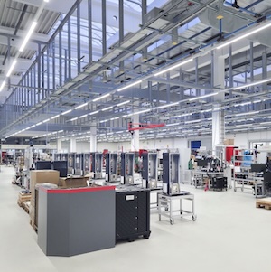
StenTech Inc., the leading multinational SMT Printing Solutions company, is pleased to announce plans to exhibit at the SMTA Guadalajara Expo, scheduled to take place Oct. 25-26, 2023 at the Expo Guadalajara in Guadalajara, Jalisco, Mexico. This year's exhibition promises to be a game-changer as StenTech unveils its latest capabilities, including a state-of-the-art laser system and award-winning Advanced Nano Coating in Booth 920.
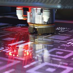
StenTech has raised the bar in the stencil manufacturing industry by making a substantial investment in the newest iteration of the StencilLaser G6080 from LPKF Laser & Electronics. This cutting-edge laser system represents a significant milestone for the SMT industry in Mexico, showcasing StenTech's unwavering commitment to its esteemed local customer base in Jalisco.
The StencilLaser G6080 stands as a flagship laser system, renowned for its best-in-class technology, tailored to meet the exacting demands of even the most discerning stencil users in the SMT industry. Distinguished by its custom carbon fiber architecture, this state-of-the-art laser system ensures superior positioning accuracy and sidewall quality while maximizing productivity. Versatile and adaptable, it is capable of cutting stainless steel and nickel stencils with material thicknesses ranging from 20 um to 1 mm (0.8 to 40 mil). StenTech's investment in this advanced laser technology empowers the company to deliver stencil solutions that consistently meet the highest industry standards.
In addition to its latest investment in state-of-the-art laser technology, StenTech's Guadalajara facility also offers an array of cutting-edge capabilities, including Advanced Nano Coating, tooling solutions, and unparalleled customer service. The combination of these advanced offerings positions StenTech as a trusted partner for the most demanding stencil projects, meeting the unique needs of its customers across various industries.
The Advanced Nano Coating features an exceptional 1-3 um hardened nano coating expertly applied to the bottom side and inside the apertures of the stencil. This cutting-edge technology offers remarkable anti-adhesion properties, effectively repelling solder flux and ensuring superior paste transfer.
By harnessing the power of StenTech's Advanced Nano Coating, transfer efficiency can soar by up to 25 percent, resulting in a substantial reduction in bridging and paste-related defects. The "non-stick" characteristics of the coating also lead to reduced underside cleaning, contributing to improved yields and decreased expenses on rework and touch-up. Additionally, stencils coated with Advanced Nano are ready for use just 30 minutes after coating, elevating production efficiency and minimizing downtime.


