










 Standard of Excellence: ‘Quality’ Is Your Company's Greatest Competitive Advantage
 Powering the Future: From Substrate to System—The Power Module Assembly
 Global Sourcing Spotlight: Global Sourcing in the Age of Constant Uncertainty





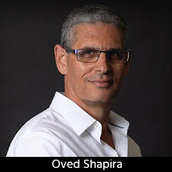
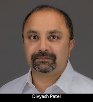
Oved Shapira is CEO of PCB Technologies, the Israeli-based printed circuit provider. PCB Technologies has recently invested in facilities and expertise to design, fabricate, and assemble substrates, a key component for advanced packaging technologies. Oved spoke with Barry Matties and Nolan Johnson about how advanced packaging will influence the industry. He said it will shift everything, including design, fabrication, assembly techniques, and capital equipment development. Some of these shifts might be subtle, and others more seismic. Whatever the changes, Oved says it’s coming.
Barry Matties: Since you joined the company, you have been instrumental in defining the direction for PCB Technologies. Could you give us an overview of the company’s current strategic direction?
Oved Shapira: When I joined the company, I first asked where we were heading and where the market was going. For our major customers, what were their projected unmet needs? I asked our CTO to talk with the CTOs of our major customers as a way to develop a multi-industrial vision with advanced technology included.
Of course, when you ask CTOs about their unmet needs, you get much feedback from different angles. When you filter out all the feedback, we found three major issues that keep repeating.
Matties: What were those issues?
Shapira: First was miniaturization. Second was heat dissipation management, which is very much connected to the miniaturization of more functionalities and the growing demand for high-power applications. The third was the registration of mixed materials.
Registration is one of the larger causes of failure on the PCB, Everything that involves multilayer and sub-lamination always has the risk of poor registration. That creates shorts or other quality issues. So, we came back to the drawing board with what we learned.
I joined after the largest private equity fund in Israel acquired the company. We had a favorable cash situation and decided to invest the capital in technologies that would serve miniaturization, heat dissipation, and registration. That’s when we built a strategy of all-in-one. You can have a PCB shop, an assembly service, and advanced packaging of multi-chip modules or SIP (system in package).
So, we upgraded the PCB shop to PCB-like substrates. Today, we can go for a pitch of 50 microns, line space of 25/25, or 20/30.
We create a unique design of organic substrates by integrating copper-moly-copper. We give them a solution for heat dissipation and heat management in combination with miniaturization. Then, we add to the substrate all our capabilities in PCBs.
To read the rest of this interview, which appeared in the September 2023 issue of PCB007 Magazine, click here.


