-

- News
- Books
Featured Books
- design007 Magazine
Latest Issues
Current Issue
Creating the Ideal Data Package
Why is it so difficult to create the ideal data package? Many of these simple errors can be alleviated by paying attention to detail—and knowing what issues to look out for. So, this month, our experts weigh in on the best practices for creating the ideal design data package for your design.

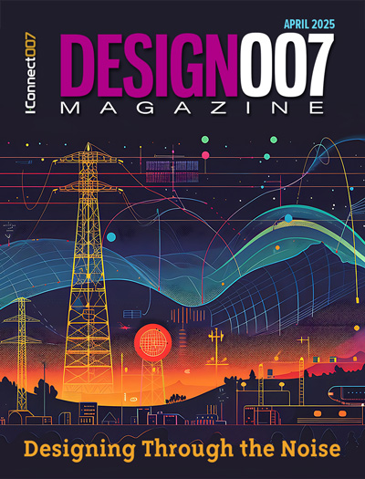
Designing Through the Noise
Our experts discuss the constantly evolving world of RF design, including the many tradeoffs, material considerations, and design tips and techniques that designers and design engineers need to know to succeed in this high-frequency realm.

Learning to Speak ‘Fab’
Our expert contributors clear up many of the miscommunication problems between PCB designers and their fab and assembly stakeholders. As you will see, a little extra planning early in the design cycle can go a long way toward maintaining open lines of communication with the fab and assembly folks.
- Articles
- Columns
Search Console
- Links
- Media kit
||| MENU - design007 Magazine
Cadence AI-Driven Multiphysics System Analysis Solution Enables Wistron to Dramatically Accelerate Product Development
December 22, 2023 | Cadence Design SystemsEstimated reading time: 1 minute
Cadence Design Systems, Inc. announced that Wistron, a leading technical service provider (TSP), has adopted and deployed the new AI-driven electromagnetic (EM) in-design analysis workflow, including the Cadence® Optimality™ Intelligent System Explorer and the Cadence Clarity™ 3D Solver, to design a complex 800G network switch. Using the Optimality Explorer’s AI-driven optimization technology and the Clarity 3D Solver for fast, accurate and scalable EM in-design analysis, Wistron was able to analyze large volumes of data—improving overall design reliability while realizing a 2X improvement in turnaround time (TAT).
Legacy 3D solvers typically deliver slower simulation results due to excessive run times and memory usage. In contrast, the Clarity 3D Solver, with its distributed multiprocessing technology and virtually unlimited capacity, quickly analyzes large and complex PCB, IC packaging and complete systems without compromising accuracy. Its exceptional performance is further fueled by the Optimality Explorer, a generative AI-driven, in-design multiphysics system analysis and optimization solution that allows design engineers to explore 3D EM and high-speed signal and power integrity results efficiently and effectively. By revealing design configurations that may not be manually achievable, the Optimality Explorer streamlines design iterations—resulting in shorter and more efficient design cycles.
“By adopting Cadence’s AI-driven optimization solution including Optimality Explorer alongside the Clarity 3D Solver for our 800G network switch and GPU server, we leveraged the design of experiments model to explore multiple simulations quickly and realized far more robust designs with a 2X improvement in TAT,” said Christopher Huang, vice president of the Enterprise and Networking Business Group at Wistron. “With a shift left of AI-enabled multiphysics systems analysis into our electronic design workflow, we are not only improving product performance but gaining valuable design insight and engineering efficiencies.”
“As high-speed electronic systems continue to grow in complexity to meet market demands, Cadence is committed to developing software solutions that address multiphysics challenges and the associated scaling demands,” said Ben Gu, corporate vice president of the Multiphysics System Analysis Group at Cadence. “Wistron has embraced the Cadence multiphysics system analysis portfolio to expedite design throughput and engineering turnaround time. The Clarity and Optimality solutions, coupled with HPC, are the trifecta for next-generation design success.”
The Clarity 3D Solver and the Optimality Explorer support Cadence’s Intelligent System Design™ strategy, which enables customers to accelerate system innovation.
Suggested Items
Imec Coordinates EU Chips Design Platform
05/09/2025 | ImecA consortium of 12 European partners, coordinated by imec, has been selected in the framework of the European Chips Act to develop the EU Chips Design Platform.
New Issue of Design007 Magazine: Are Your Data Packages Less Than Ideal?
05/09/2025 | I-Connect007 Editorial TeamWhy is it so difficult to create the ideal data package? Many of these simple errors can be alleviated by paying attention to detail—and knowing what issues to look out for. So, this month, our experts weigh in on the best practices for creating the ideal data package for your design.
RF PCB Design Tips and Tricks
05/08/2025 | Cherie Litson, EPTAC MIT CID/CID+There are many great books, videos, and information online about designing PCBs for RF circuits. A few of my favorite RF sources are Hans Rosenberg, Stephen Chavez, and Rick Hartley, but there are many more. These PCB design engineers have a very good perspective on what it takes to take an RF design from schematic concept to PCB layout.
Cadence Unveils Millennium M2000 Supercomputer with NVIDIA Blackwell Systems
05/08/2025 | Cadence Design SystemsAt its annual flagship user event, CadenceLIVE Silicon Valley 2025, Cadence announced a major expansion of its Cadence® Millennium™ Enterprise Platform with the introduction of the new Millennium M2000 Supercomputer featuring NVIDIA Blackwell systems, which delivers AI-accelerated simulation at unprecedented speed and scale across engineering and drug design workloads.
The Right Blend: Mixed Wireless Technologies
05/08/2025 | Kirsten Zima, Siemens EDAA common trend recently is to employ as many radios as possible on a single PCB. With the increase of wireless standards and the downscaling of PCB size, it can be difficult to know what the most critical design parameters are to focus on. In this article, we’ll discuss the most important considerations to make when designing with mixed wireless technologies, such as Bluetooth, GPS, and Wi-Fi, on a single PCB. These considerations include antennas, frequencies, FCC compliance, shielding, and layout with and without transition vias.


