-

-
News
News Highlights
- Books
Featured Books
- design007 Magazine
Latest Issues
Current Issue
All About That Route
Most designers favor manual routing, but today's interactive autorouters may be changing designers' minds by allowing users more direct control. In this issue, our expert contributors discuss a variety of manual and autorouting strategies.

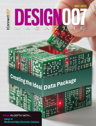
Creating the Ideal Data Package
Why is it so difficult to create the ideal data package? Many of these simple errors can be alleviated by paying attention to detail—and knowing what issues to look out for. So, this month, our experts weigh in on the best practices for creating the ideal design data package for your design.

Designing Through the Noise
Our experts discuss the constantly evolving world of RF design, including the many tradeoffs, material considerations, and design tips and techniques that designers and design engineers need to know to succeed in this high-frequency realm.
- Articles
- Columns
- Links
- Media kit
||| MENU - design007 Magazine
HDPUG: 30 Years of Collaboration
January 1, 2024 | Madan Jagernauth, Marketing Directory HDPEstimated reading time: Less than a minute
The High Density Packaging User Group International Inc. (HDP) and IPC have partnered successfully for many years. The groups signed an MoU in 2020 to strengthen this relationship, increase technical collaboration between the groups, and provide a mutual path toward emerging and disruptive high-density interconnect (HDI) technologies.
What is HDP?
HDP, founded in 1993, is a nonprofit trade organization that offers memberships to companies involved in the electronics manufacturing industry. HDP's mission is to drive innovations in the electronics industry, reducing cost and time to market through active collaborations that solve critical and emerging problems. HDP is focused on the characterization and reliability of electronic assemblies and sub-assemblies, focusing on new technologies.
This article originally appeared in the fall 2023 issue of IPC Community. To learn more about HDP’s area of focus and process, click here.
Suggested Items
Facing the Future: Investing in R&D to Stay Competitive
06/10/2025 | Prashant Patel -- Column: Facing the FutureIn the PCB industry, staying ahead of the competition requires more than production efficiency; it demands continuous innovation, a firm commitment to research and development (R&D), and a proactive approach to emerging technologies. Companies that invest in R&D are better positioned to develop advanced solutions, enhance product reliability, and adapt to the dynamic demands of the electronics industry.
UHDI Fundamentals: UHDI Drives Unique IoT Innovation—Smart Homes
06/03/2025 | Anaya Vardya, American Standard CircuitsThe combination of UHDI's high-bandwidth capabilities and IoT's real-time data processing can lead to more efficient, immersive, and smarter IoT systems. This convergence of two revolutionary technologies is enabling quantum advancements in some very “unconventional” applications.
Corning Collaborates with Broadcom to Accelerate AI Data Center Processing Capacity
05/14/2025 | BUSINESS WIRECorning Incorporated, a world leader in glass science and optical physics, today announced a collaboration with Broadcom Incorporated, a leading supplier in the semiconductor field, on a co-packaged optics (CPO) infrastructure that will significantly increase processing capacity within data centers.
Trouble in Your Tank: Organic Addition Agents in Electrolytic Copper Plating
04/15/2025 | Michael Carano -- Column: Trouble in Your TankThere are numerous factors at play in the science of electroplating or, as most often called, electrolytic plating. One critical element is the use of organic addition agents and their role in copper plating. The function and use of these chemical compounds will be explored in more detail.
Real Time with... IPC APEX EXPO 2025: Advancements for Flexible Circuit Technologies
04/11/2025 | Real Time with...IPC APEX EXPOMark Finstad and Chris Clark from Flexible Circuit Technologies discuss their new marketing campaign for catheter circuits, featuring larger formats and advanced specifications. They explain the development of in-house materials for high-density circuits, enhancing cost competitiveness. They highlight the opening of a new facility in China for advanced assembly services, along with focused training sessions to fill industry education gaps and promote early customer engagement for better project outcomes.


