


 Punching Out: How to Stay Focused in Business and M&A
 It’s Only Common Sense: Just Imagine…


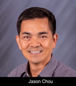
Indium Corporation Senior Area Technical Manager Jason Chou will present at the SMTA Taiwan Tech Forum on March 26 in Taoyuan City, Taiwan. Chou’s presentation will highlight the growing demand for high reliability and low-temperature solder solutions brought on by the rapidly developing electric vehicle (EV) and artificial intelligence (AI) industries.
The growing EV market is fueling demand for more sensors and power moderators. Devices used under the hood now require service temperatures up to 150°C, posing a challenge for traditional lead-free Sn-rich solder alloys, which are increasingly unsuitable for harsh environments. For AI applications, where High-Speed and High-Performance Computing (HPC) are paramount, the complexity of module packaging poses its own set of complications such as warpage-induced non-wet-opens.
Chou’s presentation will examine a novel, mixed-alloy solder technology that demonstrates the combined strengths of each constituent solder powder in the paste. This new system has proven to improve the thermal fatigue resistance of solder joints in harsh thermal cycling and thermal shock conditions. It has also been shown to reduce the reflow peak temperature from ~240°C (SAC305) to ~200–210°C.
“I believe that this new, award-winning mixed-alloy solder system provides an innovative solution to many of the challenges posed by the emergence of EV and AI technologies,” said Chou. “I look forward to sharing more about this cutting-edge solution with my industry colleagues at the SMTA Taiwan Tech Forum.”
As Senior Area Technical Manager in Taiwan, Chou provides technical support to customers with a focus on the semiconductor industry. He has 10 years of industry experience, including specialization in front-end wafer fabrication processes, thin-film modules, and defect analysis for wafer metrology. Chou earned a master’s degree in Chemistry from National Tsing Hua University and a bachelor’s degree in Chemistry from National Cheng Kung University. He served as the group leader for the National Nano Device Laboratory, Tainan, Taiwan, where he collaborated with university professors and industry professionals on special projects for semiconductor manufacturing.


