


 The Marketing Minute: AI Is Watching Your Marketing Habits
 Trouble in Your Tank: The Role of Organic Solderability Preservatives in Advanced Packaging
 It’s Only Common Sense: Lighten Up!


Whether it’s a powered prosthesis to assist a person who has lost a limb or an independent robot navigating the outside world, we are asking machines to perform increasingly complex, dynamic tasks. But the standard electric motor was designed for steady, ongoing activities like running a compressor or spinning a conveyor belt – even updated designs waste a lot of energy when making more complicated movements.
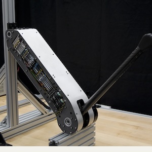
Researchers at Stanford University have invented a way to augment electric motors to make them much more efficient at performing dynamic movements through a new type of actuator, a device that uses energy to make things move. Their actuator, published March 20 in Science Robotics, uses springs and clutches to accomplish a variety of tasks with a fraction of the energy usage of a typical electric motor.
“Rather than wasting lots of electricity to just sit there humming away and generating heat, our actuator uses these clutches to achieve the very high levels of efficiency that we see from electric motors in continuous processes, without giving up on controllability and other features that make electric motors attractive,” said Steve Collins, associate professor of mechanical engineering and senior author of the paper.
Springing into action
The actuator works by harnessing the ability of springs to produce force without using energy – springs resist being stretched out and try to rebound to their natural length when released. When the actuator is, say, lowering something heavy, the researchers can engage the springs so that they stretch, taking some of the load off the motor. Then, by locking the springs in the stretched-out position, that energy can be stored to assist the motor in another task later on.
The key to engaging and disengaging the springs quickly and efficiently is a series of electroadhesive clutches. Each rubber spring is sandwiched between two clutches: one that connects the spring to the joint to assist the motor and one that locks the spring in a stretched position when it’s not being used.
These clutches consist of two electrodes – one attached to the spring and one attached to the frame or motor – that slide smoothly past each other when they aren’t active. To engage a clutch, the researchers apply a large voltage to one of its electrodes. The electrodes are drawn together with an audible click – like a faster, stronger version of the static electricity that makes a balloon stick to the wall after you rub it on carpet. Releasing the spring is as simple as grounding the electrode and dropping its voltage back to zero.
“They’re lightweight, they’re small, they’re really energy efficient, and they can be turned on and off rapidly,” said Erez Krimsky, lead author of the paper, who recently completed his PhD in Collins’ lab. “And if you have lots of clutched springs, it opens up all these exciting possibilities for how you can configure and control them to achieve interesting outcomes.”
The actuator built by Collins and Krimsky has a motor augmented with six identical clutched springs, which can be engaged in any combination. The researchers ran the design through a series of challenging motion tests that included rapid acceleration, changing loads, and smooth, steady movement. At every task, the augmented motor used at least 50 percent less power than a standard electric motor and, in the best case, reduced power consumption by 97 percent.
Motors that can do more
With significantly more efficient motors, robots could travel further and accomplish more. A robot that can run for a full day, instead of only an hour or two before needing to recharge, has the potential to undertake much more meaningful tasks. And there are plenty of unsafe situations – involving toxic materials, hazardous environments, or other dangers – where we would much prefer to send a robot than risk a person.
“This has implications for assistive devices like prosthetics or exoskeletons as well,” Krimsky said. “If you don’t need to constantly recharge them, they can have a more significant impact for the people that use them.”
Currently, it takes a few minutes for the actuator’s controller to calculate the most efficient way to use the combination of springs to accomplish a brand new task, but the researchers have plans to shorten that timeframe considerably. They envision a system that can learn from previous tasks, creating a growing database of increasingly efficient movements and using artificial intelligence to intuit how to effectively accomplish something new.
“There are a bunch of little control and design tweaks we’d like to make, but we think that the technology is really at a place where it’s ready for commercial translation,” Collins said. “We’d be excited to try to spin this out from the lab and start a company to begin making these actuators for the robots of the future.”


