-

-
News
News Highlights
- Books
Featured Books
- smt007 Magazine
Latest Issues
Current Issue
Spotlight on Mexico
Mexico isn’t just part of the electronics manufacturing conversation—it’s leading it. From growing investments to cross-border collaborations, Mexico is fast becoming the center of electronics in North America. This issue includes bilingual content, with all feature articles available in both English and Spanish.

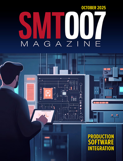
Production Software Integration
EMS companies need advanced software systems to thrive and compete. But these systems require significant effort to integrate and deploy. What is the reality, and how can we make it easier for everyone?

Spotlight on India
We invite you on a virtual tour of India’s thriving ecosystem, guided by the Global Electronics Association’s India office staff, who share their insights into the region’s growth and opportunities.
- Articles
- Columns
- Links
- Media kit
||| MENU - smt007 Magazine
Chiplet Architecture for AI Will Create New Demands for Assembly
May 28, 2024 | Nolan Johnson, SMT007 MagazineEstimated reading time: 2 minutes
As we examine the entire AI ecosystem more closely, it becomes clear that AI algorithms are intensely hungry for compute power. This demand is accelerating beyond the customary rate predicted by Moore’s Law, just as traditional semiconductor fabrication methods are failing to maintain Moore’s Law. It’s a real dilemma.
Those watching AI say that advanced packaging techniques, which have been in R&D development for some time, see AI as their killer app. AI is needed to propel these cutting-edge packages into the mainstream.
At a 2022 symposium on advanced packaging in Washington, D.C., I met Dale McHerron, a researcher on AI compute hardware. As we discussed IBM’s work in this area, Dale introduced me to Arvind Kumar, a principal research scientist and manager in AI hardware and chiplet architectures.
I reached out to Arvind to discuss his keynote presentation at the recent IMAPS conference where he discussed the AI hardware ecosystem and role of advanced packaging. Those in the assembly services industry know that any new packages will require accurate and reliable placement on the EMS manufacturing floor. Arvind shares his perspective and some predictions based on his research. It is also clear there is still much coordination and communication needed to make this work.
Nolan Johnson: What is chiplet architecture and why does it matter? How is advanced packaging moving forward?
Arvind Kumar: Chiplet architectures, which allow the partitioning of complex designs into tightly co-packaged sub-elements, are influencing the way we think about packaging. We would like to put more chips into a single package and have them talk to each other with high bandwidth, low latency, and low-energy interconnects. That goal is driving emerging packaging technologies to higher interconnect densities, more routing layers, and larger body sizes.
Johnson: Ever since semiconductors were developed, we’ve used the thought pattern of making bigger monolithic chips. Why the change?
Kumar: For a long time, the fundamental idea was that we could get more performance out of larger dies at the most advanced technology node. Fabricating all parts of a chip at the most advanced node is getting very expensive and has major yield challenges, so this drives us toward smaller die sizes. Additionally, we can partition the chip such that some parts that don’t scale well can remain in an older technology node. That's a very natural fit for chiplet architecture.
To continue reading this interview that originally appeared in the May 2024 issue of SMT007 Magazine, click here.
Testimonial
"Our marketing partnership with I-Connect007 is already delivering. Just a day after our press release went live, we received a direct inquiry about our updated products!"
Rachael Temple - AlltematedSuggested Items
I-Connect007 Editor’s Choice: Five Must-Reads for the Week
10/31/2025 | Nolan Johnson, I-Connect007Last week, the IMPACT conference took place in Taipei, bringing together advanced packaging experts from around the globe to share their knowledge. We’ll be bringing you post-conference coverage over the next few weeks, so look for that in our newsletters, and in the Advanced Electronic Packaging Digest. Other news seemed to have the U.S. at the center of the global discussions. My picks start in Phoenix, where TSMC, NVIDIA, and Amkor are all scrambling to establish new capabilities. There’s nothing like a strong demand signal to cause build-out, and AI chips are doing exactly that.
Nvidia’s Blackwell Chips Made in Arizona Still Head to Taiwan for Final Assembly
10/27/2025 | I-Connect007 Editorial TeamNvidia has begun production of its next-generation Blackwell GPUs in the United States, but the company still depends heavily on Taiwan to complete the process, The Register reported.
TSMC Fast-Tracks Advanced Chip Technology at Arizona Plant Amid Rising AI Demand
10/27/2025 | I-Connect007 Editorial TeamTSMC said earlier this month that it’s speeding up the rollout of its most advanced chip technology in the US because of rising AI product demand and Intel’s growing competition, The Register reported.
YES Selected to Deliver Full Portfolio of Advanced Packaging Tools for Glass Panel AI and HPC Applications
10/24/2025 | BUSINESS WIREYield Engineering Systems (YES), a leading provider of advanced process equipment for AI and high-performance computing (HPC) semiconductor applications, announced that it has received multiple tool orders from a global leader in AI infrastructure solutions.
TSMC Reports Third Quarter EPS of NT$17.44
10/22/2025 | TSMCTSMC announced consolidated revenue of NT$989.92 billion, net income of NT$452.30 billion, and diluted earnings per share of NT$17.44 (US$2.92 per ADR unit) for the third quarter ended September 30, 2025.


