


 Global PCB Connections: Let the Spec Fit the Board, Not Just the Brand
 Beyond Design: Refining Design Constraints
 The Pulse: Design Constraints for the Next Generation


Samsung Reportedly Achieves Technical Breakthrough, Stacking 3D DRAM to 16 Layers
June 5, 2024 | PRNewswireEstimated reading time: 1 minute
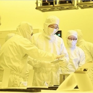
According to the news report from DIGITIMES Asia, Samsung Electronics has successfully stacked the next-gen 3D DRAM to 16 layers, twice as many as its competitor Micron.
According to reports from TheElec and ZDNet Korea, citing industry sources, Samsung has successfully stacked 3D DRAM into 16 layers. In contrast, Micron has only achieved 8 layers. However, the 3D DRAM product is currently in the feasibility stage; the goal is to realize commercialization by 2030.
The 3D DRAM uses vertical stacking, which can increase the capacity per unit area by three times, thus enabling the rapid processing of large amounts of data. Samsung aims to widen the gap with competitors in 3D DRAM technology. Compared to existing DRAM structures, 3D DRAM can include more storage cells and reduce electrical interference.
Unlike traditional DRAM, the VS-CAT style 3D DRAM is expected to be manufactured by combining two wafers, a concept similar to YMTC's Xtacking. 3D DRAM stacking is also expected to utilize Wafer-to-Wafer (W2W) hybrid bonding, a technology already utilized in NAND and CMOS Image Sensors (CIS).
At the same time, Samsung is also researching vertical channel transistor (VCT) style 3D DRAM. The industry also refers to VCT-style 3D DRAM as 4F SQUARE, with its most notable characteristic being its vertically oriented transistor structure. If Samsung successfully develops this, the die area could shrink to around 30% of the original size.
Industry sources indicated that Samsung will unveil 4F SQUARE prototypes in 2025. In contrast, Samsung's two major competitors in the DRAM market, SK Hynix and Micron have elected to develop 3D technology with a stacked cell style.
In addition, Samsung mentioned the possibility of applying Backside Power Delivery Network (BSPDN) technology to DRAM for the first time. BSPDN is considered a highly difficult technology, and Samsung plans to introduce BSPDN technology into the 2nm process by 2025.
Share on:


Suggested Items
Transition Between DRAM Generations Drives Diverging 3Q25 Price Trends; Consumer DDR4 Prices Expected to Surge Over 40%
07/07/2025 | TrendForceTrendForce’s latest findings show that the three major DRAM suppliers are shifting capacity toward high-end products and have begun announcing end-of-life (EOL) plans for PC and server-grade DDR4 and mobile LPDDR4X.
Micron, Trump Administration Announce Expanded U.S. Investments in Leading-Edge DRAM Manufacturing and R&D
06/12/2025 | MicronMicron Technology, Inc. and the Trump Administration have announced Micron’s plans to expand its U.S. investments to approximately $150 billion in domestic memory manufacturing and $50 billion in R&D, creating an estimated 90,000 direct and indirect jobs. Micron's plan is to bring advanced HBM packaging capabilities to the United States. In addition, Micron has finalized a $275 million CHIPS Act direct funding award supporting its investment to expand and modernize its Manassas, Virginia facility, which will begin this year. This investment will onshore Micron’s 1-alpha DRAM node, reinforcing the company’s ongoing commitment to key sectors including industrial, automotive, defense and aerospace, and medical devices.
DRAM Revenue Drops 5.5% in the First Quarter of 2025; SK hynix Overtakes Samsung for Top Spot
06/03/2025 | TrendForceTrendForce’s latest findings reveal that global revenue for the DRAM industry reached US$27.01 billion in 1Q25, marking a 5.5% QoQ decline. This downturn was driven by falling contract prices for conventional DRAM and a contraction in HBM shipment volumes.
Downstream Inventory Reduction Eases DRAM Price Decline in 2Q25
03/25/2025 | TrendForceTrendForce’s latest findings reveal that U.S. tariff hikes prompted most downstream brands to frontload shipments to 1Q25, accelerating inventory reduction across the memory supply chain.
Server DRAM and HBM Continue to Drive Growth, 4Q24 DRAM Industry Revenue Increases by 9.9% QoQ
02/28/2025 | TrendForceTrendForce’s latest research reveals that global DRAM industry revenue surpassed US$28 billion in 4Q24, marking a 9.9% QoQ increase. This growth was primarily driven by rising contract prices for server DDR5 and concentrated shipments of HBM, leading to continued revenue expansion for the top three DRAM suppliers.