


 Dan’s Biz Bookshelf: ‘The Next RenAIssance: AI and the Expansion of Human Potential’
 The Chemical Connection: When the Industry Moves Faster Than the Standards
 Driving Innovation: Selecting the Right Laser Source


BOOK EXCERPT: The Printed Circuit Assembler’s Guide to... Encapsulating Sustainability for Electronics, Chapter 3
July 24, 2024 | I-Connect007 Editorial TeamEstimated reading time: 2 minutes
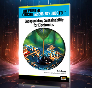
The Printed Circuit Assembler’s Guide to... Encapsulating Sustainability for Electronics, by Beth Turner, MacDermid Alpha Electronics Solutions
Chapter 3: Industry Sectors and Relevant Test Methods
General Purpose
General purpose encapsulation resins are suited to a wide range of applications where protection and electrical insulation are required. Typically, they show good flow and self-levelling properties to completely encapsulate all components. Good flow properties are important to prevent air entrapment that can occur when the viscosity is so high that air is unable to escape. The pot life, working life, and gel time can vary greatly from product to product. Pot life measurements are useful to understand how a mixed system is likely to flow when dispensed into a unit. Both the general-purpose epoxy (GPE) and polyurethane typically show good initial flow properties and are suited to most potting applications. The general-purpose polyurethane (GPP) shows a lower mixed system viscosity, so might be more suited to applications with tight spacing between components or leads. The pot life of the GPE is longer, meaning it will retain its workable and flow properties for more time.
Good adhesion is essential to completely seal a module. Adhesion to wires, leads, terminals, and housing materials is required for complete physical protection against deleterious fluids and other contaminants. As the popularity of portable and wearable electronics continues to rise, everyday devices must be able to tolerate exposure to dust and moisture, thus ruggedized performance is essential for both indoor and outdoor environments. Ingress protection (IP) ratings describe protection against solids and liquids. To achieve any decent level of protection at a system level, an encapsulation resin must adhere appropriately to the substrates to which it is applied.
Lap shear strength testing is a useful method to compare adhesive strength on different substrates. Test methods such as ASTM D1002 (metals) and ASTM D3163 (plastics) provide a useful framework to compare the adhesive performance of encapsulation resins, evaluate effectiveness of surface preparation techniques, and assess durability of bonded substrates in different environments. The test procedure involves bonding two identical surfaces into a single lap joint and applying shear stress until rupture occurs. The load at failure and type of failure is recorded and the shear strength at failure can then be calculated. Both the GPE and GPP typically show good adhesion to most substrates including those commonly used as housing materials. They do show some limitations when it comes to difficult substrates, including untreated PET. Specialist grade encapsulants are required for certain low surface energy substrates.
Share on:


Subscribe
Stay ahead of the technologies shaping the future of electronics with our latest newsletter, Advanced Electronics Packaging Digest. Get expert insights on advanced packaging, materials, and system-level innovation, delivered straight to your inbox.Subscribe now to stay informed, competitive, and connected.
Suggested Items
EDIP Opens the Door: EU Funding Now Available for Defence Electronics Including PCBs and Substrates
04/21/2026 | Alison James and Chris Mitchell, Global Electronics AssociationThe European Commission has published a call for proposals under the European Defence Industry Programme (EDIP), and for European electronics manufacturers the message is clear: this is real money for real capacity, and PCBs and IC substrates are explicitly in scope. EDIP's Industrial Reinforcement Actions (IRA) dedicate €122.25 million to key electronic components, covering guidance electronics, propulsion electronics, RF and laser modules, multispectral cameras, avionics, PCBs and IC substrates, lithium-ion polymer batteries, power electronics, and critical semiconductor building blocks
IC Substrates vs. UHDI: The Future of Interconnect
03/15/2026 | Marcy LaRont, I-Connect007Advanced packaging is driving feature sizes below 50 microns, forcing IC substrates and UHDI PCBs into overlapping territory. Following his presentation at the Pan-European Design Conference (PEDC) in January, Jan Pedersen, director of technology at NCAB Group, spoke with us about how heterogeneous integration, evolving HDI roadmaps, and supply chain pressures are shaping the next phase of advanced packaging.
UHDI, AI, and RF Materials: Signals From the Next Phase of Advanced Packaging
03/11/2026 | I-Connect007The upcoming issue of Advanced Electronics Packaging Digest explores several developments shaping the future of advanced electronics, from the convergence of IC substrates and ultra-high-density interconnect (UHDI) PCBs to the growing influence of artificial intelligence on semiconductor packaging and the materials science behind high-frequency system performance.
Ibiden Approves ¥500 Billion Electronics Investment, Expands IC Substrate Capacity at Ono Plant
02/27/2026 | IBIDENIbiden Co., Ltd. announced that its Board of Directors has approved a capital investment plan totaling approximately ¥500 billion for its electronics business over the three-year period from fiscal year 2026 through fiscal year 2028.
KYZEN to Showcase MICRONOX Power Electronics Cleaning Chemistries at IMAPS Device Packaging Conference 2026
02/13/2026 | KYZEN'KYZEN, the global leader in innovative environmentally responsible cleaning chemistries, will exhibit at the International Symposium on Microelectronics (IMAPS) International Conference and Exhibition on Device Packaging scheduled to take place March 2-5 at the Sheraton Grand at Wild Horse Pass in Phoenix, AZ.