


 Fresh PCB Concepts: Resilience and Renewal in Domestic PCB Manufacturing
 Designers Notebook: Power and Ground Distribution Basics
 Elementary, Mr. Watson: Heat—The Hidden Villain of Power Electronics


Imec Achieves Record-low Charge Noise for Si MOS Quantum Dots Fabricated on a 300mm CMOS Platform
July 30, 2024 | ImecEstimated reading time: 3 minutes
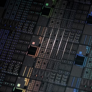
Imec, a world-leading research and innovation hub in nanoelectronics and digital technologies, announced the demonstration of high quality 300mm-Si-based quantum dot spin qubit processing with devices resulting in a statistically relevant, average charge noise of 0.6µeV/√ Hz at 1Hz. In view of noise performance, the values obtained are the lowest charge noise values achieved on a 300mm fab-compatible platform. Such low noise values enable high-fidelity qubit control, as reducing the noise is critical for maintaining quantum coherence and high fidelity control. By demonstrating those values, repeatedly and reproducibly, on a 300mm Si MOS quantum dot process, this work makes large-scale quantum computers based on Si quantum dots a realistic possibility.
Si quantum dot spin qubits are promising building blocks to realize large-scale quantum computers for two main reasons. First, Si spin qubits with long quantum coherence times (a metric reflecting their ability to store quantum information for a long time) and high-fidelity quantum gate operations have been repeatedly demonstrated in lab environments and are therefore a well-established and tested technology with realistic prospects. Second, and potentially more importantly for the long-term viability, the underlying technology is compatible and intimately linked with CMOS manufacturing technologies and as such offers the possibility of wafer-scale uniformity and yield with the required advanced back-end-of-line interconnection of the Si quantum dot structures that are needed for truly large scale quantum chips, with millions or even billions of qubits operating in synchrony.
Several types of Si quantum dot spin qubits exist and are being pursued at imec. In this work, the quantum dot spin qubits were defined by metal-oxide-semiconductor (MOS) quantum dot structures that resemble modified transistor structures to trap a single spin of an electron or hole. To achieve long quantum coherence times, the noise, and in particular the charge noise of the quantum dot should be as low as possible. That noise generally results from residual charges, trapped nearby or even inside the quantum dot, removing those is key to increase the performance of the spin qubits. Ultimately, this is determined by the full processing stack of the quantum dot qubit structure, since any defects introduced there need to be minimized. While this can be realized through lab-based techniques such as very gentle lift-off processes that reduce process damage, industrial manufacturing techniques like subtractive etch and lithography-based patterning have shown to easily result in degradation of the device and interface quality, particularly at the Si/SiO2 interface nearby the quantum dot qubits. As a result, the charge noise of Si/SiO2-based quantum dot structures manufactured in professional fabrication facilities is typically higher than the values obtained using lab-based processing.
By careful optimization and engineering of the 300mm Si/SiO2-based MOS gate stack, imec achieved a record-low average charge noise level of only 0.6µeV/√ Hz (at 1Hz), across 300 mm wafers and characterized using statistical methods. Kristiaan De Greve, imec Fellow and Program Director Quantum Computing at imec: “We demonstrated charge noise levels that, depending on the source, are between half an order of magnitude to one order of magnitude lower, when compared to current state-of-the-art fab-based Si quantum dot structures and achieved remarkably uniform quantum dot operation. Our results confirm that 300mm Si MOS is a compelling material platform for quantum dot spin qubits and highlight the maturity of industrial fabrication techniques for qubit development.”
In addition, the statistical analysis methods used to characterize the low charge noise devices revealed fundamental insights into their origin. “Knowing the source of the charge noise will give us directions to further optimize the quantum dot structures,” De Greve adds. “The low-noise qubit environment and demonstrated uniformity of the CMOS manufacturing are just the start of a series of enabling technology developments for upscaling quantum chips towards eventual practical quantum computing, which, with current understanding, will require millions of physical qubits.”
Share on:


Testimonial
"Advertising in PCB007 Magazine has been a great way to showcase our bare board testers to the right audience. The I-Connect007 team makes the process smooth and professional. We’re proud to be featured in such a trusted publication."
Klaus Koziol - atgSuggested Items
Keysight Advances Quantum Engineering with New System-Level Simulation Solution
10/30/2025 | BUSINESS WIREKeysight Technologies, Inc. announced the release of Quantum System Analysis, a breakthrough Electronic Design Automation (EDA) solution that enables quantum engineers to simulate and optimize quantum systems at the system level.
Global Electronics Association Unveils Powerhouse Tech and Innovation Keynote Speakers for APEX EXPO 2026
10/29/2025 | Global Electronics AssociationThe Global Electronics Association announces its APEX EXPO keynote lineup, featuring industry titans exploring the frontiers of quantum computing, artificial intelligence, and the electrification of global industries.
Imec Sets Electro-Optic Performance Record in Thin-Film Strontium Titanate at Cryogenic Temperatures
10/27/2025 | ImecAt 4 degrees Kelvin, most electro-optic materials falter. Nanoelectronics R&D center imec has now successfully engineered thin-film strontium titanate (SrTiO₃) that delivers record electro-optic performance with low optical loss, pointing to shorter, faster building blocks for quantum devices.
SemiQon's Cryogenic Chip Technology for Quantum Computing and Space Applications Receives Award from EARTO
10/17/2025 | PRNewswireEARTO, the organisation of the European Research and Technology Organisations, awarded SemiQon and VTT first prize in the "Impact Expected" category on 14 October 2025 in Brussels for a pioneering cryogenic CMOS (complementary metal-oxide semiconductor) chip innovation.
SemiQon's Cryogenic Chip Technology for Quantum Computing and Space Applications Receives Award from EARTO
10/16/2025 | PRNewswireEARTO, the organisation of the European Research and Technology Organisations, awarded SemiQon and VTT first prize in the "Impact Expected" category on 14 October 2025 in Brussels for a pioneering cryogenic CMOS (complementary metal-oxide semiconductor) chip innovation.