-

- News
- Books
Featured Books
- smt007 Magazine
Latest Issues
Current Issue
Moving Forward With Confidence
In this issue, we focus on sales and quoting, workforce training, new IPC leadership in the U.S. and Canada, the effects of tariffs, CFX standards, and much more—all designed to provide perspective as you move through the cloud bank of today's shifting economic market.

Intelligent Test and Inspection
Are you ready to explore the cutting-edge advancements shaping the electronics manufacturing industry? The May 2025 issue of SMT007 Magazine is packed with insights, innovations, and expert perspectives that you won’t want to miss.

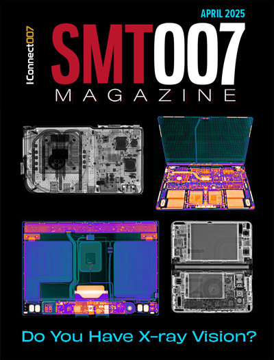
Do You Have X-ray Vision?
Has X-ray’s time finally come in electronics manufacturing? Join us in this issue of SMT007 Magazine, where we answer this question and others to bring more efficiency to your bottom line.
- Articles
- Columns
Search Console
- Links
- Media kit
||| MENU - smt007 Magazine
Navigating Cost Drivers and Sustainability in PCB Production: A Comprehensive Guide
August 22, 2024 | Michael Marshall, NCAB GroupEstimated reading time: 2 minutes
In May, I had the privilege of presenting "Cost Drivers in PCB Production" to attendees at the SMTA Wisconsin Expo. This presentation, one of our most popular, received tremendous feedback, inspiring us to share our insights more broadly through a comprehensive white paper on the subject.
One of my favorite examples to share from this white paper which really illustrates the impact of both cost and sustainability is panel utilization. Utilization is the percentage of the working panel allocated to the specific array. Pricing is based on the entire working panel. If you have a PCB that takes up two-thirds of a panel, there is not enough space left on the panel to fit a second board but you still pay for all the wasted material. In addition, this results in excess material waste.
Consider these three panel options below. We can see the large waste strips (or wasted area) in panelization 1. In panelization 2 and 3 we have removed these waste areas. The smaller array allows more boards per panel and helps keep a high material utilization and also a low material demand.
In these examples, panelization 3 is the lowest cost option. It has the same composition as the actual PCB but ends up in the recycling bin after the PCB is depaneled. Option 1 is a very common request however it comes at a premium and increased waste over option 3 which has a higher panel utilization and also a smaller material demand due to the reduced number of smaller rails.
This visual is a tangible example of cost driver and sustainability impact, and how they can relate to one another. In this white paper we dive into more than 20 examples categorized into two types: hard cost drivers and soft cost drivers, providing insights into their impacts and effective management strategies, while also keeping in mind the aspects that contribute to the sustainability impacts of a PCB.
Hard cost drivers encompass direct, tangible costs that are quantifiable and associated with the physical aspects of a project. These costs are typically straightforward to estimate and track, making them critical components of project budgeting. In the white paper, we break down aspects like board size, layer count, and via types
Soft cost drivers, on the other hand, are indirect costs related to the electrical design, engineering analysis, drafting, and modeling. Hiring skilled professionals, using advanced design software, and conducting feasibility studies are integral to this phase. While these costs are not directly tied to physical components, they are essential for ensuring that the project’s feasibility, safety and adherence to desired specifications.
We invite you to explore this detailed article on cost drivers and sustainability impacts, helping you get your design right from the start. You can download the full Cost Drivers white paper here.
Michael Marshall is a field application engineer at NCAB Group.
Suggested Items
Nordson Electronics Solutions Develops Panel-level Packaging Solution for Powertech Technology, Inc. That Achieves Yields Greater Than 99% for Underfilling During Semiconductor Manufacturing
06/11/2025 | Nordson Electronics SolutionsNordson Electronics Solutions, a global leader in reliable electronics manufacturing technologies, has developed several solutions for panel-level packaging (PLP) during semiconductor manufacturing. In one particular case, Nordson’s customer, Powertech Technology, Inc. (PTI) saw underfill yields improve to greater than 99% as they plan to transition from wafers to panels in their manufacturing operations. edwd
Japan’s Sharp to Sell LCD Plant to Taiwanese Parent Company Foxconn
05/14/2025 | I-Connect007Japanese electronics firm Sharp Corp. announced on May 12 that it plans to sell its Kameyama No. 2 liquid crystal display plant to its Taiwanese parent company, Foxconn.
Panel Driver IC Price Decline Slows in 1H25; Gold Prices, China Subsidies, and U.S.-China Tariffs Emerge as Key Variables
04/28/2025 | TrendForceTrendForce’s latest investigation finds that China’s subsidy policies and rising concerns over reciprocal tariffs are reshaping brand strategies in the panel market, indirectly influencing price trends for panel driver ICs.
Tandem Panel Shipments to Jump Again to 36% in 2026
04/25/2025 | BUSINESS WIREAccording to recent display industry research from Omdia, tandem RGB penetration into the OLED tablet and notebook panel markets surged from almost zero to more than 30% in 2024.
QD-OLED to Account for 73% of OLED Monitor Shipments in 2025, Driven by Advancing Technology and New Products
04/16/2025 | TrendForceTrendForce’s latest investigations reveal that ongoing advancements in OLED displays are propelling the growth of QD-OLED monitor shipments. QD-OLED’s share of OLED monitor shipments is expected to rise from 68% in 2024 to 73% in 2025, highlighting its strong competitiveness in the high-end monitor market.


