


 Marcy’s Musings: Setting the Pace for an Industry in Motion
 It’s Only Common Sense: We Have Met the Enemy, and It’s Us
 Dan’s Biz Bookshelf: ‘Super Performance: 8 Strategies to Reach Full Potential’


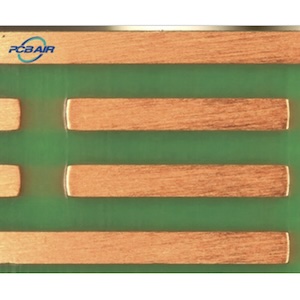
From Silicon to Systems
September 10, 2024 | Andy Shaughnessy, Design007 MagazineEstimated reading time: 2 minutes
For the past few years, IPC has been championing the term “silicon to systems.” More than a buzzword, it has become a slogan—and even a kind of roadmap—for the organization. The term comes in especially handy when IPC is advocating for this industry in Washington, D.C., often addressing politicians who have little understanding of electronics technology.
But what does silicon to systems mean to PCB designers? We asked this and more of a trio of IPC staffers: CTO Matt Kelly, Chief Strategist for Advanced Packaging Devan Iyer, and design instructor Kris Moyer, CID+. Does your company take a silicon-to-systems approach to design?
Andy Shaughnessy: Matt, what do you mean by silicon to systems?
Matt Kelly: The term silicon to systems was born in our IPC Advanced Packaging report in the fall of 2021. It was a notion that I used to try to simplify the breadth and the scope of everything that was going on at the time, and is still going on today, of course. A lot of the focus with the CHIPS Act in the United States, Europe, and other geographies has really revolved around the step function changes that are occurring with semiconductors and electronics packaging. This comes out in terms of the U.S. CHIPS Act in the design of those chips, the architectures, and the fact that Moore's Law has been running out of economic steam for quite some time.
Silicon to systems was really a way for us to go beyond the discussion of just the semiconductor and the packaging of that chip. It's very important because everything follows silicon. We are at the beginning of a 10-plus-year period of significant disruption because of this technology change and adoption. Silicon to systems is basically a way of saying, “You don't hold a chip in your hand.” You don't even hold a component in your hand; you hold a cellphone in your hand, and for that system to work, while these components and changes are absolutely important, it's really just one part among many more that makes up the system you are using.
It’s basically about having a very circumspect view, not just looking at your own silo. From a design perspective, all these new systems can be across any application while they're being dreamt up by the OEMs, with increased functionality and density, and all these great things that we're trying to do all in single devices. This is really being powered by these chip technologies. I know Devan has a lot to say in this area as well.
Devan Iyer: Thanks, Matt. I think that's a good start. Speaking of silicon to systems, this also includes the non-silicon devices like gallium nitride. If you really look at high-speed devices or high-power devices like silicon carbide or EV automotive applications, they’re outside the domain of silicon, but you can call that chip to systems or silicon to systems. Semiconductor to systems might be a more accurate term.
To read the entire article, which originally published in the September 2024 Design007 Magazine, click here.
Share on:


Testimonial
"Your magazines are a great platform for people to exchange knowledge. Thank you for the work that you do."
Simon Khesin - Schmoll MaschinenSuggested Items
Designers Notebook: Heterogeneous Interposer Design Challenge, Part 1
01/19/2026 | Vern Solberg -- Column: Designer's NotebookThe development of monolithic (system-on-chip) ICs revolutionized the electronics industry, enabling the creation of heterogeneous products by integrating multiple active elements within the same silicon base, which includes a central processing unit (CPU), memory functions, sensors, and communication tasks.
Cadence Launches Partner Ecosystem to Accelerate Chiplet Time to Market
01/12/2026 | Cadence Design SystemsCadence announced a Chiplet Spec-to-Packaged Parts ecosystem to reduce engineering complexity and accelerate time to market for customers developing chiplets targeting physical AI, data center, and high-performance computing (HPC) applications.
Cadence Celebrates 20 Years in Pune, Reinforces Long-Term R&D Commitment
01/07/2026 | Cadence Design SystemsCadence, a global leader in electronic system design, is celebrating 20 years in Pune as a core research and development hub.
onsemi to Develop Next-Generation GaN Power Devices with GlobalFoundries
01/05/2026 | onsemionsemi announced it has signed a collaboration agreement with GlobalFoundries (GF) to develop and manufacture advanced gallium nitride (GaN) power products using GF’s state-of-the-art 200mm eMode GaN-on-silicon process, starting with 650V.
Pan-European Electronics Design Conference Returns to Prague in January
12/31/2025 | Global Electronics AssociationThe Pan-European Electronics Design Conference is jointly hosted and organized by the Electronics Design and Manufacturing Association (FED) and the Global Electronics Association – two associations representing more than 3,700 companies from the electronics industry.