-

- News
- Books
Featured Books
- smt007 Magazine
Latest Issues
Current Issue
Spotlight on Mexico
Mexico isn’t just part of the electronics manufacturing conversation—it’s leading it. From growing investments to cross-border collaborations, Mexico is fast becoming the center of electronics in North America. This issue includes bilingual content, with all feature articles available in both English and Spanish.

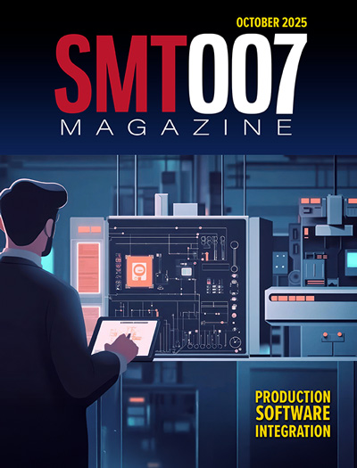
Production Software Integration
EMS companies need advanced software systems to thrive and compete. But these systems require significant effort to integrate and deploy. What is the reality, and how can we make it easier for everyone?

Spotlight on India
We invite you on a virtual tour of India’s thriving ecosystem, guided by the Global Electronics Association’s India office staff, who share their insights into the region’s growth and opportunities.
- Articles
Article Highlights
- Columns
- Links
- Media kit
||| MENU - smt007 Magazine
Silicon to Systems: Collaboration Between IC and PCB Design Continues
October 2, 2024 | Andy Shaughnessy, Design007Estimated reading time: 1 minute
The walls are coming down between the designers of chips and PCBs. Because of the complexity of electronic systems, IC designers and PCB designers are increasingly finding themselves in need of information from technologists upstream and downstream, from silicon through the system level.
Stephen Chavez, senior product marketing manager at Siemens, shares his thoughts on this silicon-to-systems approach and what it means for PCB designers, EDA tool providers, and system-level developers as well.
More technologists are pointing out the need for PCB designers to focus on silicon-to-systems. What does that term mean to you and to EDA companies like Siemens?
Stephen Chavez: Silicon-to-systems refers to a holistic approach in electronics design where the interaction and integration of silicon (ICs, chips) are considered all the way through to the system level (PCBs, full electronic products). For EDA companies like Siemens, this means developing tools and methodologies that support seamless design flows from the chip level up to the complete system. This approach ensures that all components work together efficiently, reduces design iterations, and improves time-to-market by addressing potential integration issues early in the design process.
What do PCB designers need to understand about silicon and packages?
PCB designers must understand the following aspects of silicon and packages:
- Signal integrity and power integrity: As signals travel from silicon through the package to the PCB, maintaining signal quality and managing power distribution is critical. PCB designers must account for high-speed signal requirements, impedance control, and proper power delivery network design to avoid noise in regard to crosstalk, EMI, and EMC.
- Thermal management: Higher integration and power densities in silicon and packages lead to heat generation. Designers must incorporate effective thermal management solutions, such as heat sinks, thermal vias, and appropriate material choices.
- Land patterns and layout considerations: Understanding the physical and electrical requirements of IC packages is crucial. This includes correct pin mapping, accommodating different package types (e.g., BGA, LGA, microBGAs, QFP, etc.), and ensuring sufficient spacing and layer stackup to include the necessary via technologies to support the chip's needs.
- Design for manufacturing: Awareness of the manufacturing processes for both silicon and PCB can help designers create designs that are easier to manufacture, test, and assemble, reducing costs and time. Close collaboration with your external suppliers is key to success.
To read the rest of this article in the September 2024 issue of Design007 Magazine, click here.
Testimonial
"We’re proud to call I-Connect007 a trusted partner. Their innovative approach and industry insight made our podcast collaboration a success by connecting us with the right audience and delivering real results."
Julia McCaffrey - NCAB GroupSuggested Items
WestDev Announces Advanced Thermal Analysis Integration for Pulsonix PCB Design Suite
10/29/2025 | WestDev Ltd.Pulsonix, the industry-leading PCB design software from WestDev Ltd., announced a major enhancement to its design ecosystem: a direct interface between Pulsonix and ADAM Research's TRM (Thermal Risk Management) analysis software.
Connect the Dots: Designing for the Reality of UHDI PCBs—Drilling
11/04/2025 | Matt Stevenson -- Column: Connect the DotsUltra high density interconnect (UHDI) PCBs are changing the game in designing for the reality of manufacturing. With both consumer and industrial electronic devices becoming more advanced, the demand for UHDI PCBs will grow. That means we’re all likely to be designing more UHDI boards. UHDI advanced miniaturization technology challenges designers with regard to both board thickness and footprint. Designers will face more variables in every aspect of design creation. This is certainly the case with drilling.
The Shaughnessy Report: Watt About Power Integrity?
10/08/2025 | Andy Shaughnessy -- Column: The Shaughnessy ReportYes, that headline is the equivalent of a dad joke, but editors can’t pass up a chance to inject a little humor into a headline, and I had to take my shot. Power integrity (PI) problems are no joke. Current power demands are increasing, especially with AI, 5G, and EV chips, which can lead to voltage drops that kill your performance.
New Fil Arzola Class: Designing for the Future, and for Sustainability
10/07/2025 | Andy Shaughnessy, I-Connect007If you have not yet taken a class from Fil Arzola, you are missing out. In late October, Fil will be teaching the class "Building Sustainable Model-Based PCBs," speaking from the design perspective. I had the pleasure of catching this course at last year's IPC APEX EXPO, and I walked away with a lot to think about. I asked Fil to discuss his upcoming course. Registration is open now.
American Standard Circuits to Exhibit at SMTA International
10/06/2025 | American Standard CircuitsAnaya Vardya, President, and CEO of American Standard Circuits/ASC Sunstone Circuits has announced that his company will once again exhibit at SMTA International 2025 to be held at the Donald E Stephens Convention Center in Rosemont, Illinois on October 19th through the 23rd, 2025.


