


 Fresh PCB Concepts: Resilience and Renewal in Domestic PCB Manufacturing
 Designers Notebook: Power and Ground Distribution Basics
 Elementary, Mr. Watson: Heat—The Hidden Villain of Power Electronics


NEOTech Announces Implementation of Enhanced Wire Bonding Process to Boost Microelectronics Manufacturing Efficiency
October 8, 2024 | NEOTechEstimated reading time: 3 minutes
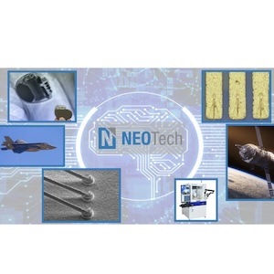
NEOTech, a leading provider of electronic manufacturing services (EMS), design engineering, and supply chain solutions in the high-tech industrial, medical device, and aerospace/defense markets, is excited to announce the recent implementation of an enhanced wire bonding manufacturing process for microelectronics circuit assemblies. This innovative process significantly increases production yields while reducing the production cycle time for each assembly. NEOTech remains committed to continuous improvements, particularly in the manufacturing of extraordinarily high-tech microelectronics products for the nation’s leading OEMs in the Aerospace & Defense, Medical Device, and Industrial markets. As part of this commitment, NEOTech has researched, tested, and qualified an advanced wire bonding technique known as Standoff Stitch (SOS), which further reinforces the company’s dedication to delivering high-quality, precision-driven solutions.
NEOTech, already recognized as an industry leader in SMT electronics manufacturing, stands at the forefront of high-tech microelectronics circuit assembly as well. The company’s original first-pass yields for wire bond and bond pull test processes were already excellent, achieving a 99.3% success rate. However, for mission-critical electronics used in aerospace, defense, space, and medical implantable device applications, even this high yield rate required further improvement. Common methods to enhance wire bond yield and reliability, such as the Burnishing process and the Security Bonding process, have been effective but significantly increase production time. To address this challenge, NEOTech has researched and implemented the SOS wire bond process, which not only boosts reliability but also reduces the production cycle time, offering a more efficient solution without compromising quality.
The SOS wire bond process is a superior method for ensuring high-quality interconnects of micro fine wires to the conductive pads on the substrate surface, which are often uneven or wavy due to the screen-printing process. When standard wire bonding methods are applied to these uneven surfaces, poor bond adherence can result, impacting overall quality. The SOS process addresses this issue by incorporating a gold ball approximately 2.5 mil in diameter during the first step of the wire bonding process. This gold ball accommodates the uneven surfaces without the need for additional steps, significantly reducing production time for each assembly. Furthermore, the increased surface area at the substrate bond interface created by the gold ball forms a more robust bond, enhancing reliability. NEOTech has seen remarkable improvements from this method, with production yields increasing to 99.99% and throughput doubling.
Jim Doyle, Chief Executive Officer of NEOTech’s Aerospace & Defense Business, expressed his enthusiasm for the recent advancements, stating, “At NEOTech, we are dedicated to fostering a culture of continuous improvement to ensure we consistently deliver the highest quality products to our customers. The implementation of the SOS wire bonding process is a testament to our commitment to innovation and operational excellence. By enhancing our wire bonding capabilities, we not only improve production efficiency but also ensure the reliability and performance of mission-critical microelectronics for the aerospace, defense, medical, and industrial sectors. We are proud of our team’s unwavering focus on quality and their efforts to push the boundaries of what’s possible in electronics manufacturing.”
NEOTech distinguishes itself through its broad capabilities and exceptional service offerings, serving industries such as aerospace/defense, medical devices, industrial, and high-tech sectors. Renowned for delivering high-quality products and solutions, NEOTech has become a trusted partner for complex, mission-critical electronic manufacturing projects. The company’s cutting-edge facilities and advanced manufacturing technologies guarantee precision and reliability in every product. NEOTech’s commitment to quality is evident through its adherence to stringent standards, backed by certifications like ISO 9001:2015, ISO 13485:2016, and AS9100.
At the core of NEOTech’s success is its customer-centric approach. Offering a comprehensive suite of services — from design and prototyping to full-scale production and post-production support — NEOTech tailors its solutions to meet each customer’s specific needs. The company’s ability to provide personalized solutions, while also reducing time-to-market and optimizing costs, has earned it a strong reputation for delivering exceptional value.
Share on:


Testimonial
"Our marketing partnership with I-Connect007 is already delivering. Just a day after our press release went live, we received a direct inquiry about our updated products!"
Rachael Temple - AlltematedSuggested Items
Unlocking the Promise of AI in Electronics Manufacturing
10/29/2025 | Shobhit Agrawal, Keysight TechnologiesThe electronics manufacturing industry is rapidly evolving as more complicated products are introduced in the production lines, which require technological advancements even in the production processes. The requirements for production that is efficient, product quality that is greater, and product life cycles that are shorter are more crucial than ever before. In the electronic device life cycle, from design to maintenance, test phases have a significant impact on the economy of the company. Test processes are closely linked to the production volume and impacted by the complexity of the product. For businesses to maintain their competitive edge, they need to adopt innovative solutions and redefine processes.
Driving Innovation: Mechanical and Optical Processes During Rigid-flex Production
10/28/2025 | Kurt Palmer -- Column: Driving InnovationRigid-flex printed circuit boards are a highly effective solution for placing complex circuitry in tight, three-dimensional spaces. They are now indispensable across a range of industries, from medical devices and aerospace to advanced consumer electronics, helping designers make the most efficient use of available space. However, their unique construction—combining rigid and flexible materials—presents a fundamental challenge for PCB manufacturers.
SMTAI 2025 Review: Reflecting on a Pragmatic and Forward-looking Industry
10/27/2025 | Marcy LaRont, I-Connect007Leaving the show floor on the final afternoon of SMTA International last week in Rosemont, Illinois, it was clear that the show remains a grounded, technically driven event that delivers a solid program, good networking, and an easy space to commune with industry colleagues and meet with customers.
The Marketing Minute: Marketing With Layers
10/15/2025 | Brittany Martin -- Column: The Marketing MinuteMarketing to a technical audience is like crafting a multilayer board: Each layer serves a purpose, from the surface story to the buried detail that keeps everything connected. At I-Connect007, we’ve learned that the best marketing campaigns aren’t built linearly; they’re layered. A campaign might start with a highly technical resource, such as an in-depth article, a white paper, or a podcast featuring an engineer delving into the details of a process. That’s the foundation, the substance that earns credibility.
Taking Control of PCB Verification One Step at a Time
10/09/2025 | Kirk Fabbri, Siemens EDAToday’s designs are as complex as ever, and engineers face tough decisions every day. Simulation and verification teams are confronted with a three-fold challenge: understanding the underlying theory, mastering the tools, and applying best practices.Engineers need to navigate a vast and ever-changing cast of design and simulation tools, often with overlapping functionality.