-

- News
- Books
Featured Books
- smt007 Magazine
Latest Issues
Current Issue
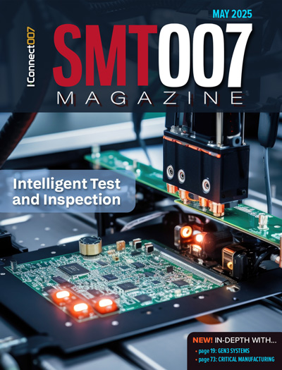
Intelligent Test and Inspection
Are you ready to explore the cutting-edge advancements shaping the electronics manufacturing industry? The May 2025 issue of SMT007 Magazine is packed with insights, innovations, and expert perspectives that you won’t want to miss.

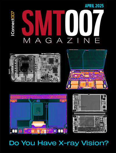
Do You Have X-ray Vision?
Has X-ray’s time finally come in electronics manufacturing? Join us in this issue of SMT007 Magazine, where we answer this question and others to bring more efficiency to your bottom line.

IPC APEX EXPO 2025: A Preview
It’s that time again. If you’re going to Anaheim for IPC APEX EXPO 2025, we’ll see you there. In the meantime, consider this issue of SMT007 Magazine to be your golden ticket to planning the show.
- Articles
- Columns
Search Console
- Links
- Media kit
||| MENU - smt007 Magazine
MKS’ Atotech and ESI to Participate at TPCA Show & IMPACT Conference 2024
October 23, 2024 | MKS Instruments, Inc.Estimated reading time: 4 minutes
MKS Instruments, Inc., a global provider of enabling technologies that transform our world, announced that its strategic brands ESI (laser systems) and Atotech (process chemicals, equipment, software, and services) will showcase their latest range of leading manufacturing solutions for printed circuit board (PCB) and package substrate manufacturing at the upcoming 25th Taiwan Circuit Board Industry International Exhibition 2024 to be held at the Taipei Nangang Exhibition Center from 23-25 October 2024.
Combining leading capabilities in lasers, optics, motion, process chemistry, and equipment, MKS is uniquely positioned to Optimize the InterconnectSM, a key enabler for the next generation of advanced electronics, which represents the next frontier in miniaturization and complexity. The Optimize the InterconnectSM approach demonstrates the company’s unique position to support the development of next-generation advanced PCB and package substrate manufacturing solutions for its customers and partners. “Our commitment to APAC is more than strategic, it is fundamental to our future. We are partnering with key manufacturers and supporting new technologies and ever smaller feature sizes by combining MKS’ ESI laser drilling technologies with MKS’ Atotech chemistry and plating equipment,” said Jim Schreiner, EVP and COO, MSD.”
The company has recently installed the latest equipment and process technology at its local APAC technology centers to drive the production of next generation package substrates and offer customers and OEMs faster development cycles for new products and materials, enabling high-end SAP technology requiring <=5/5µm lines and spaces.
Another example of progress comes from applications such as flex, advanced HDI or substrate-like PCBs. MKS can offer customers a comprehensive combination of optimized laser drilling, plating and surface modification chemistries and manufacturing equipment. Customers benefit from our unique one-stop-shop destination for pre-treatment, via formation, plating, and final finishing with fast turnaround times that don’t require production interruption, enabling our customers to achieve better yields, productivity, and performance. For substrate-like PCBs, MKS’ Atotech and ESI are currently working together with the industry to enable the next generation of mSAP technology and to introduce more sustainable solutions to comply with CO2 footprint reduction roadmaps, said Harald Ahnert, VP and GM Chemistry, MSD.
Wayne Cole, Senior VP, Global Sales and Service, adds, “As technology advances, semiconductors, package substrates and printed circuit boards continue to play a key role in driving innovation across multiple industries. These components are essential for powering next generation communication networks, enabling high-performance computing, supporting electrification in vehicles and advancements in driver assistance systems to pave the way towards sustainable transportation. These technologies are the foundation for a more connected and sustainable future. We are committed to meeting the evolving needs of our customers by delivering cutting-edge solutions that push the boundaries of electronics design. Experts from both brands will be available and ready to discuss latest industry trends and challenges at the TPCA Show booth K-915 on the 1st floor of the Nangang Exhibition Hall 1”.
On the chemistry side, highlights in surface treatment include EcoFlash® S300, a new differential etch solution suitable for advanced package substrates and , our new high-tech inner-layer adhesion promoter for high-speed AI applications. For metallization, our highlights include Printoganth® MV TP2, a high performance electroless copper process specifically designed for SAP fine line applications, and our even more enhanced Printoganth® MV TP3 process, which enables ultra-thin Cu deposition for fine lines down to 2/2 µm L/S, ideally combined with Cupraganth® MV, our new and revolutionary copper-based activation system. For electrolytic copper plating, we highlight our new reverse pulse plating solution for inclusion-free, high aspect ratio through hole filling of package substrate cores, Inpulse® 2THF2, and our production-proven InPro® SAP3 process for BMV filling with best surface distribution at high current densities. For conformal high hole density package substrate core plating we are promoting Cuprapulse® XP7-IN, our new solution for excellent plating uniformity.
For final finishing highlights range from the OSP solution OS-Tech® SIT 2, the new Aurotech® G-Bond 3 versatile gold bath for nickel/gold, nickel/palladium/gold and palladium/gold plating to Stannatech® for flex PCBs, as well as for thick tin plating of µ-LEDs or solder depot plating and Stannatech® IC for package substrates.
PCB equipment systems promotions include G-Plate®, a new HVM tool for PTH processes of next generation package substrates enabling highest yields and cutting-edge fine line capability targeting L/S <5/5 µm, vPlate®, a new vertical continuous plating tool for advanced HDI and package substrate for best-in-class surface uniformity. And last not least the new Uniplate®, the company’s flagship HVM system and industry-leading horizontal plating equipment for next-generation HDI PCBs and package substrate manufacturing.
Laser equipment promotions include the latest Capstone™, a high-performance/throughput breakthrough productivity for flex PCB UV drilling and Geode™ (CO2 and UV laser for HDI and package substrate applications). A special show highlight Geode™ A our new CO2 laser system for high precision and high-speed ABF build-up laminate processing. Geode™ G2 our new CO2 laser system for high-precision and high-speed HDI and mSAP via drilling. The Geode™ platform provides 15% higher optical transmission, 21% less total service area and up to 65% lower power consumption.
Suggested Items
Elephantech: For a Greener Tomorrow
04/16/2025 | Marcy LaRont, PCB007 MagazineNobuhiko Okamoto is the global sales and marketing manager for Elephantech Inc., a Japanese startup with a vision to make electronics more sustainable. The company is developing a metal inkjet technology that can print directly on the substrate and then give it a copper thickness by plating. In this interview, he discusses this novel technology's environmental advantages, as well as its potential benefits for the PCB manufacturing and semiconductor packaging segments.
Trouble in Your Tank: Organic Addition Agents in Electrolytic Copper Plating
04/15/2025 | Michael Carano -- Column: Trouble in Your TankThere are numerous factors at play in the science of electroplating or, as most often called, electrolytic plating. One critical element is the use of organic addition agents and their role in copper plating. The function and use of these chemical compounds will be explored in more detail.
Real Time with... IPC APEX EXPO 2025: MKS' Atotech—Leading Innovations in Semiconductor Solutions
03/28/2025 | Real Time with...IPC APEX EXPOIn this interview, Marcy LaRont speaks with Kuldip Johal, CTO, MKS’ Atotech. Based in Boston, MKS operates in vacuum solutions, photonics, and specifically for the Atotech division, material solutions. MKS significantly impacts the semiconductor industry, supplying components for up to 85% of global semiconductor tools and covers processes and materials for 70% of PCB manufacturing steps.
Gold as a Key Component in PCBs and IC Substrates
03/20/2025 | Britta Schafsteller, Sandra Nelle, and Kuldip Johal, MKS' AtotechGold has long been a cornerstone in the electronics industry, particularly in the surface finishing of PCBs and IC substrates. It provides essential surface protection while enabling various assembling techniques, such as soldering connections and wire bonding, using aluminum, gold, or copper wires.
PCB007 Magazine: The Essential Guide to Surface Finishes—March 2025
03/17/2025 | I-Connect007 Editorial TeamIn the March 2025 issue of PCB007 Magazine, we go back to basics, recount a little history, and look forward to addressing the many challenges that high density, high frequency, adhesion, SI, and corrosion concerns for harsh environments bring to the fore.


