-

- News
- Books
Featured Books
- pcb007 Magazine
Latest Issues
Current Issue
Alternate Metallization Processes
Traditional electroless copper and electroless copper immersion gold have been primary PCB plating methods for decades. But alternative plating metals and processes have been introduced over the past few years as miniaturization and advanced packaging continue to develop.
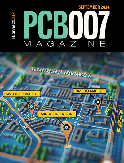
Technology Roadmaps
In this issue of PCB007 Magazine, we discuss technology roadmaps and what they mean for our businesses, providing context to the all-important question: What is my company’s technology roadmap?
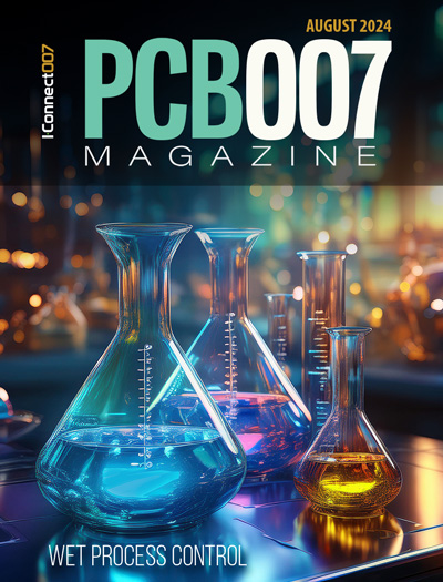
Wet Process Control
In this issue, we examine wet processes and how to obtain a better degree of control that allows usable data to guide our decisions and produce consistently higher-quality products.
- Articles
- Columns
Search Console
- Links
- Media kit
||| MENU - pcb007 Magazine
Unlocking Advanced Circuitry Through Liquid Metal Ink
October 31, 2024 | I-Connect007 Editorial TeamEstimated reading time: 1 minute
PCB UHDI technologist John Johnson of American Standard Circuits discusses the evolving landscape of electronics manufacturing and the critical role of innovation, specifically liquid metal ink technology, as an alternate process to traditional metallization in PCB fabrication to achieve ever finer features and tighter tolerances. The discussion highlights the benefits of reliability, efficiency, and yields as a tradeoff to any increased cost to run the process. As this technology becomes better understood and accepted, even sought out by customers and designers, John says there is a move toward mainstream incorporation.
Nolan Johnson: John, what is liquid metal ink technology?
John Johnson: It is a chemistry developed by LDQX (formerly Averatek) as part of its licensed solution for doing A-SAP™. Liquid Metal Ink (LMI™) is the heart of this process. The A-SAP process involves putting down a thin plating of electroless copper which forms the base of subsequent plate-ups for traces and so forth. You generate all your ultra-fine line circuitry with LMI. It is a non-aqueous substance that carries a palladium complex in solution. It can be coated through a dip method, a spray method, and other ways. At ASC, we use the dip method.
The beauty is that the LMI is key to the whole process. The palladium that's created is a very dense coating. It is a very unique approach. It touches atom to atom and is several atoms thick. It is semi-aqueous so it wets well, getting down into the small micro-topography that would be left behind if you had etched copper foil. The chemical bond to the copper foil is not significant, roughly only a 10% contribution to the total adhesion. Your adhesion comes from being able to coat on that micro-topography and plate it up with the right electroless. You get very good adhesion for a variety of different materials.
Nolan Johnson: If the chemical bond to copper is about a 10% contributor to adhesion, how much does the palladium affect adhesion?
John Johnson: With palladium there is no real chemical adhesion that takes place as the laminate is already cured, but it is important for adhesion in the subsequent processing.
To read this entire conversation, which appeared in the October 2024 issue of PCB007 Magazine, click here.
Suggested Items
Atotech to Participate at KPCA Show 2024
09/03/2024 | AtotechMKS’ Atotech will participate in this year’s KPCA Show 2024 in Incheon, held at Songdo Convensia from September 4-6, 2024.
Real Time with… THECA 2024: State of the Art Copper Adhesion
08/09/2024 | Real Time with... THECABruce Lee, MacDermid Alpha Electronics Solutions, joined Nolan Johnson following his paper presentation on the show's mainstage. Lee provided a detailed overview of the current state of adhesion promoters and discussed the interaction between mechanical adhesion, chemical adhesion, signal integrity, and substrate impacts.
MKS’ Atotech to Participate at Semicon Europa 2022
11/02/2022 | AtotechMKS’ Atotech will be exhibiting at Semicon Europa and present its latest results on Cu-to-Cu direct bonding for 3D integration during Advanced Packaging Solutions Conference (APC) in Munich on November 16 from 11:50 a.m. – 12:10 p.m. (room 14c; presenter: Ralf Schmidt, R&D Manager Semiconductor).
Trouble in Your Tank: Success in Photolithography Starts With Surface Preparation
11/09/2022 | Michael Carano -- Column: Trouble in Your TankThe photolithography process defines the circuitry on the panel. As one may surmise, the imaging process used in the fabrication of high density and ultra high-density circuity has made significant advances over the last decade—and just in time. With finer lines and spaces as well as more attention to fabrication of printed wiring advanced packaging substrates. However, as is so true of many of the processes in PWB fabrication, up and down stream processes can and will influence what happens in a particular process.
MacDermid Alpha Launches ALPHA HiTech AD13-9910B Ultra-Low Temperature Adhesive
08/11/2022 | MacDermid Alpha Electronics SolutionsMacDermid Alpha Electronics Solutions, a global supplier of integrated solutions from our Circuitry, Assembly and Semiconductor divisions, announces the launch of ALPHA HiTech AD13-9910B ultra-low temperature adhesive, designed to mitigate defects on very temperature sensitive parts and substrates.

