-

- News
- Books
Featured Books
- design007 Magazine
Latest Issues
Current Issue
Rules of Thumb
This month, we delve into rules of thumb—which ones work, which ones should be avoided. Rules of thumb are everywhere, but there may be hundreds of rules of thumb for PCB design. How do we separate the wheat from the chaff, so to speak?

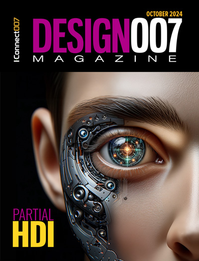
Partial HDI
Our expert contributors provide a complete, detailed view of partial HDI this month. Most experienced PCB designers can start using this approach right away, but you need to know these tips, tricks and techniques first.

Silicon to Systems: From Soup to Nuts
This month, we asked our expert contributors to weigh in on silicon to systems—what it means to PCB designers and design engineers, EDA companies, and the rest of the PCB supply chain... from soup to nuts.
- Articles
- Columns
Search Console
- Links
- Media kit
||| MENU - design007 Magazine
Estimated reading time: 3 minutes
Nolan’s Notes: Soldering Technologies
The QWERTY keyboard is an anachronism, yet it is ubiquitous. It was conceived in the early 1870s by Christopher Latham Sholes, and finalized by the Remington Company in 1878 for use in mechanical typewriters. It’s 150 years later and that keyboard layout is still arguably the primary interface to our data-driven world. Other keyboard layouts—the Dvorak, for example—are reputed to be more efficient, faster, and given to less hand strain. But QWERTY, with all its foibles, persists, relegating the other keyboards to niche status. Quirks and all, no one can deny that the QWERTY keyboard gets the job done, and well enough that the world resists the change.
There are schools of thought that soldering methods are similarly anachronistic but still useful enough not to be worth changing. While that may be true, I see that soldering technologies are experiencing significant changes. It might not be apparent on the surface, but changes are afoot, and there are some disruptive things underway as well.
Photonic soldering, for example, provides capabilities that traditional methods don’t. Traditional technologies are also adding capabilities, responding to changing market needs.
Now, it seems simple and obvious that if component packaging trends weren’t shifting, soldering technologies would not need to adapt. BGAs are getting huge. Recently, I was discussing the 100 mm and larger BGAs with a CEO of an EMS provider, and he said the joke is that some of these components are bigger than some of the boards going through the shop. Funny, but true. His observation was that if the line could place the part, then soldering wasn’t an issue. Thermal coefficients and coplanarity issues, however, are growing concerns. Going the other direction, passives are becoming microscopic and LEDs are so small they’re difficult to handle.
We lead off the December 2024 issue of SMT007 Magazine with an interview with Stan Farnsworth of PulseForge, who shares an example of how a photonic system can handle those very small LED arrays. Our cover image is just one example of how photonic soldering can tackle applications traditional soldering methodologies would struggle with. Is photonic soldering the Dvorak keyboard of the soldering world? Today, maybe. But the future remains to be seen.
I’ve also heard that large hardware companies, such as Google and Amazon, are encouraging the use of vacuum in convection ovens to eliminate voids. The story is that this technique increases yields and reduces the device's power consumption. In the cellphone market alone, femtowatts of power reduction per phone accumulates across billions of phones to represent a (positive) disruptive drop in power consumption. Disruptive solutions can come from small improvements as well as innovative new technologies. Dr. Paul Wild of Rehm Thermal Systems examines the solder quality benefits of using vacuum and condensation methods in appropriate applications.
Mike Konrad’s column delivers an interview with Dr. Nava Shpaisman, strategic collaboration manager at KLA, on advanced packaging technologies coming out of semiconductor. Some folks in the EMS provider space have stated that they don’t see why semiconductor packaging work matters to EMS companies. I would respond that such an opinion is short-sighted. Read Mike’s interview (and our coverage of advanced packaging and heterogeneous integration over the past couple of years) carefully. The changes will put stress upon pick-and-place at both extremes, large and small; surface planarity will become a key issue to yields. Substrate materials will change. Identical packages with even more configurations will stress component management and MES systems. The power and heat management these chips require will change bills of materials and assembly processes in new ways. These methods will move into our basic consumer microprocessors. Even photonic interconnects are moving to the high-performance chips—now that’s definitely disruptive. If you’re an EMS supplier, you will be affected; that’s why we cover the topic.
Soldering is the heartbeat of assembly, and new developments are taking place to match the rest of the innovation in electronics. It’s certain we will revisit these topics again, so let us know what you want to read about. We constantly ask, “What do we want our readers to learn?” but what we value most is when you tell us what you want to read. I look forward to hearing from you.
This column originally appeared in the December 2024 issue of SMT007 Magazine.
More Columns from Nolan's Notes
Nolan's Notes: The Rise (and Risk) of Data‘Deepfake’ Components
Solder Printing: A 1:1 Ratio of Technical and Creative
Nolan’s Notes: What It Means to Thrive
Nolan’s Notes: Plenty to Say About Certification
Nolan’s Notes: The Changing EMS Landscape
Nolan’s Notes: Coming to Terms With AI
Nolan’s Notes: Do More, Get More


