-

- News
- Books
Featured Books
- smt007 Magazine
Latest Issues
Current Issue
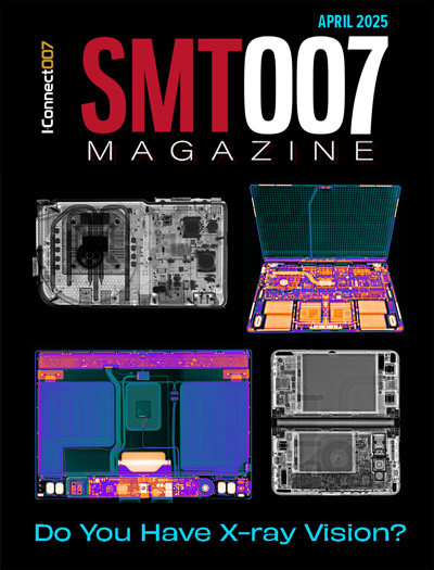
Do You Have X-ray Vision?
Has X-ray’s time finally come in electronics manufacturing? Join us in this issue of SMT007 Magazine, where we answer this question and others to bring more efficiency to your bottom line.

IPC APEX EXPO 2025: A Preview
It’s that time again. If you’re going to Anaheim for IPC APEX EXPO 2025, we’ll see you there. In the meantime, consider this issue of SMT007 Magazine to be your golden ticket to planning the show.

Technical Resources
Key industry organizations–all with knowledge sharing as a part of their mission–share their technical repositories in this issue of SMT007 Magazine. Where can you find information critical to your work? Odds are, right here.
- Articles
Article Highlights
- Columns
Search Console
- Links
- Media kit
||| MENU - smt007 Magazine
Imec Achieves Breakthrough in Silicon Photonics
January 13, 2025 | ImecEstimated reading time: 2 minutes
Imec, a world-leading research and innovation hub in nanoelectronics and digital technologies, has announced a significant milestone in silicon photonics with the successful demonstration of electrically-driven GaAs-based multi-quantum-well nano-ridge laser diodes fully, monolithically fabricated on 300 mm silicon wafers in its CMOS pilot prototyping line. Achieving room-temperature continuous-wave lasing with threshold currents as low as 5 mA and output powers exceeding 1 mW, the results, detailed in last week’s Nature publication, demonstrate the potential of direct epitaxial growth of high-quality III-V materials on silicon. This breakthrough provides a pathway to the development of cost-effective, high-performance optical devices for applications in data communications, machine learning and artificial intelligence.
The lack of highly scalable, native CMOS-integrated light sources has been a major roadblock for the widespread adoption of silicon photonics. Hybrid or heterogeneous integration solutions, such as flip-chip, micro-transfer printing or die-to-wafer bonding, involve complex bonding processes or the need for expensive III-V substrates which are often discarded after processing. This not only increases costs but also raises concerns about sustainability and resource efficiency. For that reason, the direct epitaxial growth of high-quality III-V optical gain materials selectively on large-size silicon photonics wafers remains a highly sought-after objective.
The large mismatch in crystal lattice parameters and thermal expansion coefficients between III-V and Si materials inevitably initiates the formation of crystal misfit defects, which are known to deteriorate laser performance and reliability. Selective-area growth (SAG) combined with aspect-ratio trapping (ART) significantly reduces defects in III-V materials integrated on silicon by confining misfit dislocations within narrow trenches etched in a dielectric mask.
“Over the past years, imec has pioneered nano-ridge engineering, a technique that builds on SAG and ART to grow low-defectivity III-V nano-ridges outside the trenches. This approach not only further reduces defects but also enables precise control over material dimensions and composition. Our optimized nano-ridge structures typically feature threading dislocation densities well below 105 cm-2. Now, imec exploited the III-V nano-ridge engineering concept to demonstrate the first full wafer-scale fabrication of electrically pumped GaAs-based lasers on standard 300 mm silicon wafers, entirely within a CMOS pilot manufacturing line,” says Bernardette Kunert, scientific director at imec.
Leveraging the low-defectivity GaAs nano-ridge structures, the lasers integrate InGaAs multiple quantum wells (MQWs) as the optical gain region, embedded in an in-situ doped p-i-n diode and passivated with an InGaP capping layer. Achieving room-temperature, continuous-wave operation with electrical injection is a major advancement, overcoming challenges in current delivery and interface engineering. The devices show lasing at ~1020 nm with threshold currents as low as 5 mA, slope efficiencies up to 0.5 W/A, and optical powers reaching 1.75 mW, showcasing a scalable pathway for high-performance silicon-integrated light sources.
“The cost-effective integration of high-quality III-V gain materials on large-diameter Si wafers is a key enabler for next-generation silicon photonics applications. These exciting nano-ridge laser results represent a significant milestone in using direct epitaxial growth for monolithic III-V integration. This project is part of a larger pathfinding mission at imec to advance III-V integration processes towards higher technological readiness, from flip-chip and transfer-printing hybrid techniques in the near term, over heterogeneous wafer- and die-bonding technologies and eventually direct epitaxial growth in the longer term,” states Joris Van Campenhout, fellow silicon photonics and director of the industry-affiliation R&D program on Optical I/O at imec.
Suggested Items
STMicroelectronics Details Company-Wide Program to Reshape Manufacturing Footprint and Resize Global Cost Base
04/14/2025 | STMicroelectronicsSTMicroelectronics N.V., a global semiconductor leader serving customers across the spectrum of electronics applications, disclosed further elements of its program to reshape its global manufacturing footprint.
IEEE Study Leverages Silicon Photonics for Scalable and Sustainable AI Hardware
04/14/2025 | PRNewswireThe emergence of AI has profoundly transformed numerous industries. Driven by deep learning technology and Big Data, AI requires significant processing power for training its models. While the existing AI infrastructure relies on graphical processing units (GPUs), the substantial processing demands and energy expenses associated with its operation remain key challenges.
TSMC, ASE Join Forces with 100+ Companies to Drive Silicon Photonics Technology Integration
04/11/2025 | SEMIThe SEMI Silicon Photonics Industry Alliance (SiPhIA) held the Bridging Light & Silicon: SEMI SiPhIA SIGs Kick-off & Seminar today, announcing the official launch of three Special Interest Groups (SIGs) aimed at integrating expertise from various sectors to formulate industry standards and accelerate technological innovation and commercialization.
DuPont Enhances Optical Silicone Technical Capabilities in Taiwan
04/07/2025 | DuPontDuPont announced the enhancement and expansion of its Optical Silicone Lab at its Taoyuan site in Taiwan.
Teradyne Announces Production System for Double-Sided Wafer Probe Test for Silicon Photonics
04/02/2025 | TeradyneTeradyne, a leading provider of automated test equipment, has partnered with ficonTEC, a global leader in production solutions for photonics assembly and test, to announce the availability of the first high-volume, double-sided wafer probe test cell for silicon photonics.


