-

- News
- Books
Featured Books
- smt007 Magazine
Latest Issues
Current Issue
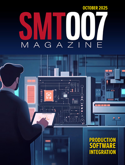
Production Software Integration
EMS companies need advanced software systems to thrive and compete. But these systems require significant effort to integrate and deploy. What is the reality, and how can we make it easier for everyone?

Spotlight on India
We invite you on a virtual tour of India’s thriving ecosystem, guided by the Global Electronics Association’s India office staff, who share their insights into the region’s growth and opportunities.

Supply Chain Strategies
A successful brand is built on strong customer relationships—anchored by a well-orchestrated supply chain at its core. This month, we look at how managing your supply chain directly influences customer perception.
- Articles
- Columns
- Links
- Media kit
||| MENU - smt007 Magazine
EDA Tools and the Designer of the Future
January 28, 2025 | Andy Shaughnessy, Design007 MagazineEstimated reading time: 1 minute
We’re seeing new, young technologists moving into the PCB design and design engineering segment, and it’s just in time; many veteran designers are headed to retirement.
At the same time, there have been various recent advances in EDA tools. What will the PCB designer’s job—and the designer’s software tools—look like in the next five years?
Bob Potock, vice president of marketing for Zuken USA, weighs in on the PCB designers of tomorrow, and the EDA tools that will take them into an evermore complex future.
Andy Shaughnessy: I imagine Zuken has a “profile” of its typical user. How do you see this their job and its requirements evolving over the next few years?
Bob Potock: At Zuken, we believe that the PCB design and layout market is evolving. Today’s tools are mature, powerful, and easy to use. However, what's changing in the design process is how the tools are used and by whom. The standard hand-off from the design engineer to the PCB layout designer is becoming a thing of the past. A board with average complexity is more commonly designed, placed, and routed by the same individual: the hardware engineer. The modern hardware engineer will be an electrical engineer who can learn how to do PCB layout on the job. Moderately complex board designs now and in the future will see the traditional PCB layout function moving to the hardware engineer.
The high-complexity PCB market is different. The tools are more powerful, and the designs have more critical requirements. IC packaging may become part of the PCB layout activity at this complexity level. The traditional design engineer hand-off to the PCB layout designer may still exist. However, this modern PCB layout designer is an electrical engineer with training in power integrity, signal integrity, manufacturing, and IC packaging.
To read this entire conversation, which appeared in the January 2025 issue of Design007 Magazine, click here.
Testimonial
"We’re proud to call I-Connect007 a trusted partner. Their innovative approach and industry insight made our podcast collaboration a success by connecting us with the right audience and delivering real results."
Julia McCaffrey - NCAB GroupSuggested Items
NCAB Reports Continued Growth in Order Intake and Net Sales in Q3 2025
10/24/2025 | NCAB GroupNCAB Group AB announced its interim report for January–September 2025, showing continued positive momentum with Q3 net sales up 6% to SEK 949 million and order intake rising 11%, driven by strong performance in key markets despite a challenging global economy.
Amphenol Reports Record Q3 2025 Results and Announces Dividend Increase
10/24/2025 | Amphenol CorporationThe Company continues to deploy its financial strength in a variety of ways to increase shareholder value. During the third quarter, the Company purchased 1.4 million shares of its common stock for $153 million and paid dividends of $201 million, resulting in total capital returned to shareholders of approximately $354 million.
MKS’ Atotech Showcases Next-gen PCB and Substrate Manufacturing Solutions at CPCA Plus 2025
10/24/2025 | MKS Inc.MKS Inc., a global provider of enabling technologies that transform our world, announced its participation in CPCA Plus Show 2025, taking place October 28 – 30 at Shenzhen International Convention and Exhibition Center.
I-Connect007 Editor’s Choice: Five Must-Reads for the Week
10/24/2025 | Andy Shaughnessy, I-Connect007This week, we have quite a bit of international content in this week’s list of must-reads. Nothing happens in a vacuum, including electronics manufacturing and design, and this has been quite an eventful year. How many of us are now tariff experts? I’m certainly not, but that hasn’t stopped me from opining about the situation.
Peters, Starteam, and Würth Elektronik Team Up For Digital Coating Technology
10/23/2025 | PetersUnder this heading, the PCB manufacturers Starteam and Würth Elektronik, along with Peters as inkjet coating supplier, have taken the initiative and worked together for months in trusting and target-oriented cooperation, to promote this innovative digital coating technology for solder resists and establish it on the market.


