-

-
News
News Highlights
- Books
Featured Books
- smt007 Magazine
Latest Issues
Current Issue
Spotlight on Mexico
Mexico isn’t just part of the electronics manufacturing conversation—it’s leading it. From growing investments to cross-border collaborations, Mexico is fast becoming the center of electronics in North America. This issue includes bilingual content, with all feature articles available in both English and Spanish.

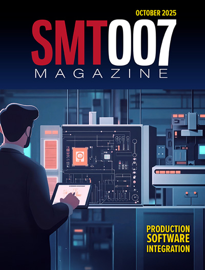
Production Software Integration
EMS companies need advanced software systems to thrive and compete. But these systems require significant effort to integrate and deploy. What is the reality, and how can we make it easier for everyone?

Spotlight on India
We invite you on a virtual tour of India’s thriving ecosystem, guided by the Global Electronics Association’s India office staff, who share their insights into the region’s growth and opportunities.
- Articles
- Columns
- Links
- Media kit
||| MENU - smt007 Magazine
Dan Beeker on the Design Engineer of the Future
February 7, 2025 | Andy Shaughnessy, Design007 MagazineEstimated reading time: 1 minute
As technical director at NXP Semiconductors, Dan Beeker specializes in EMC and signal integrity design techniques. He’s known for his field-based design classes; you may remember the cover of Meghan Trainor’s “All About That Bass” that Dan and his daughter Breezy released in 2015 titled “All About The Space.” Check it out on YouTube; it’s funny, and it definitely gets the point across.
As we begin 2025, I contacted Dan to get his thoughts about the design engineers of the future. What will their jobs look like?
Andy Shaughnessy: Dan, how will the typical PCB design engineer’s job evolve over the next five to 10 years?
Dan Beeker: The challenges will be driven by the changes in technology. Smaller IC geometries for transistors and packages and increased power supply requirements make the basic functional design more challenging. Evolving standards for reduced allowable radiated emission levels and increased levels of immunity will impact compliance.
A solid understanding of the underlying science of electromagnetic physics will be more critical than ever. Improvements in the design tool space may help, but until the tools are dielectric-aware and can manage the entire three-dimensional structure of the electronic control system, they will only provide false hope. Careful empirical evaluation of each design will still be the primary method for designing good PCBs.
To read this entire conversation, which appeared in the January 2025 issue of Design007 Magazine, click here.
Testimonial
"Advertising in PCB007 Magazine has been a great way to showcase our bare board testers to the right audience. The I-Connect007 team makes the process smooth and professional. We’re proud to be featured in such a trusted publication."
Klaus Koziol - atgSuggested Items
The Marketing Minute: Get Out of Your Lane—Electronics Marketing Needs Bold Moves
11/19/2025 | Brittany Martin -- Column: The Marketing MinuteI started skateboarding recently. It’s an unexpected hobby for someone who spends most of her day in marketing meetings, analytics dashboards, and editorial calendars. It’s awkward, humbling, and wildly out of my lane, but that’s exactly why it’s been so energizing: It forces me to redefine what I think I’m capable of.
SAICEC, Siemens to Accelerate Chip-to-Vehicle Validation Using Digital Twin Technology
11/17/2025 | SiemensSiemens announced that SAICEC, a leading provider of chip and system design services for the automotive industry, has begun building complex digital twins of automotive architectures based on Siemens’ PAVE360™ software, facilitating comprehensive verification of automotive components from system-level to chip-level.
November 2025 PCB007 Magazine: Getting to Know Our Columnists
11/17/2025 | I-Connect007 Editorial TeamThis month, PCB007 Magazine expresses gratitude to the industry columnists who share their expertise, insights, and perspectives each month. From technical innovations and process improvements to marketing and management strategies, these contributors form the backbone of our mission to educate and connect the PCB industry.
ioTech Introduces io600
11/14/2025 | ioTechAhead of productronica 2025, ioTech unveils the io600, a next-gen platform that brings intelligence, scalability, and agility to digital material deposition.
Discover the Benefits of Inkjet with Electra Polymer at Productronica 2025
11/10/2025 | Electra Polymers LtdElectra Polymers will be showcasing ElectraJet® EMJ110, our advanced low-loss inkjet soldermask, ideal for high-speed and high-frequency PCB applications, at productronica 2025.


