-

- News
- Books
Featured Books
- smt007 Magazine
Latest Issues
Current Issue
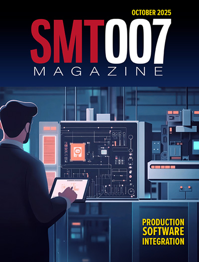
Production Software Integration
EMS companies need advanced software systems to thrive and compete. But these systems require significant effort to integrate and deploy. What is the reality, and how can we make it easier for everyone?

Spotlight on India
We invite you on a virtual tour of India’s thriving ecosystem, guided by the Global Electronics Association’s India office staff, who share their insights into the region’s growth and opportunities.

Supply Chain Strategies
A successful brand is built on strong customer relationships—anchored by a well-orchestrated supply chain at its core. This month, we look at how managing your supply chain directly influences customer perception.
- Articles
- Columns
- Links
- Media kit
||| MENU - smt007 Magazine
PCB Designers of the Future—and Their Software Tools
February 14, 2025 | Andy Shaughnessy, Design007 MagazineEstimated reading time: 1 minute
The PCB designers of tomorrow have their work cut out for them. They’ll be dealing with the continuing drive for “faster, smaller, cheaper,” while electronics become more complex. But EDA companies have improved their software tools’ capabilities over the past few years, incorporating functionalities such as AI and increasing productivity.
I asked David Wiens, product marketing manager at Siemens, to share his thoughts on the continuing evolution of PCB design and PCB designers, and how EDA software companies can help designers meet the technological requirements of tomorrow.
Andy Shaughnessy: At Siemens, I imagine you have a “profile” of your typical user. How do you see this user’s job and job requirements evolving over the next few years?
David Wiens: There is no single user persona. The larger the company, the greater the diversity of specializations/personas (e.g., design engineer, layout designer, SI specialist, manufacturing specialist, system architect, librarian, etc.). The smaller the company, the more those specializations merge (engineers in smaller teams become generalists). This stratification by engineering team size has always been there. What’s evolved over time is the roles these specialists perform.
Design engineers have had to learn about signal integrity and associated simulation tools; they’re participating more in the layout process to implement tighter performance requirements; they’ve had to learn about stack-up design; and they must consider supply chain risks when selecting components. Layout designers have had to learn about manufacturability and constraints for signal/power/thermal performance. They’ve also had to collaborate much more closely with their mechanical counterparts to achieve shrinking form factors. This evolution has meant that engineers and designers have had to work across multiple tools to get their jobs done efficiently, rather than spending all day, every day in the same tool.
To read this entire conversation, which appeared in the January 2025 issue of Design007 Magazine, click here.
Testimonial
"Your magazines are a great platform for people to exchange knowledge. Thank you for the work that you do."
Simon Khesin - Schmoll MaschinenSuggested Items
The Right Approach: Electro-Tek—A Williams Family Legacy, Part 1
10/15/2025 | Steve Williams -- Column: The Right ApproachThere is no bronze bust in the lobby or portrait in the conference room of Electro-Tek's founder—my Dad, Charles “Chuck” Williams—so with the facility closing last year after 56 years, I feel it is time to tell the story. Chuck Williams founded Electro-Tek in 1968 in our basement, eventually moving into the second floor of an old 1913 building in downtown Milwaukee that is still standing (the first of three eventual facilities).
Taiwan Rejects U.S. Proposal for 50-50 Semiconductor Production Split
10/03/2025 | I-Connect007 Editorial TeamTaiwan stated on October 1 that it will not agree to a U.S. proposal to shift half of its semiconductor production to the United States, despite mounting pressure from Washington over tariffs and chip supply security, according to Reuters.
Jiva Leading the Charge Toward Sustainable Innovation
09/30/2025 | Marcy LaRont, PCB007 MagazineEnvironmental sustainability in business—product circularity—is a high priority these days. “Circularity,” the term meant to replace “recycling,” in its simplest definition, describes a full circle life for electronic products and all their elements. The result is re-use or a near-complete reintroduction of the base materials back into the supply chain, leaving very little left for waste. For what cannot be reused productively, the ultimate hope is to have better, less harmful means of disposal and/or materials that can seamlessly and harmlessly decompose and integrate back into the natural environment. That is where Jiva and Soluboard come in.
Curing and Verification in PCB Shadow Areas
09/17/2025 | Doug Katze, DymaxDesign engineers know a simple truth that often complicates electronics manufacturing: Light doesn’t go around corners. In densely populated PCBs, adhesives and coatings often fail to fully cure in shadowed regions created by tall ICs, connectors, relays, and tight housings.
Building Electronics Excellence in India
09/08/2025 | Nolan Johnson, SMT007 MagazineFor over two decades, Dave Bergman has helped steer the Global Electronics Association’s work in India, from a single training course to a thriving regional operation with deep government and industry ties. In this interview, Dave explains how the group went from partnering with IPCA to opening its own office in 2010, creating India’s first domestic electronics manufacturing standard, and securing funding for dozens of Indian companies to attend U.S. trade shows.


