


 Knocking Down the Bone Pile: Precision Milling of Underfilled SMT Components
 Learning with Leo: Drones—Meeting Demand Without Compromise
 Nolan’s Notes: Our Spotlight on North America


TASMIT Launches Large Glass Substrate Inspection System for Advanced Semiconductor Packaging
March 4, 2025 | ACCESSWIREEstimated reading time: 2 minutes
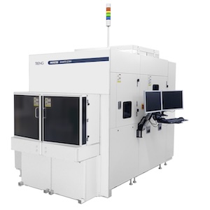
TASMIT Inc. has launched a new inspection system for glass substrates as part of its INSPECTRA® series of semiconductor wafer visual inspection systems, which has gained attention for its high efficiency in advanced semiconductor manufacturing.
The system detects not only pattern defects and foreign particles but also cracks and other defects specific to glass substrates, and is compatible with glass core interposers and rewiring glass carriers, which are used in panel level packaging (PLP) and other applications.
Semiconductor manufacturers have previously introduced inspection systems for detecting surface defects on glass substrates, but this is the industry's first system capable of inspecting both the front and back surfaces as well as the internal structure to date.
TASMIT aims to supply the large glass substrate inspection system to manufacturers of advanced semiconductors, such as PLP, targeting 1 billion yen in orders in FY2025 and 2 billion yen in FY2030.
Currently, in 2.5D packaging, a next-generation semiconductor manufacturing technology, the increasing performance of semiconductors has led to larger semiconductor chips and a higher number of chips per package due to greater integration. As a result, interposers, which serve as intermediate components that electrically connect the chips to the substrate, are also being scaled up.
Traditionally, silicon interposers made from 12-inch silicon wafers have been used, but since wafers are circular, the number of chips that can be produced from a single wafer is limited, making it difficult to meet growing demand. As an alternative, glass substrates are gaining attention as they can be manufactured in large substrate sizes and are suitable for high-density packaging, this new system is compatible with industry-standard 650mm square glass substrates.
However, as glass is prone to microscopic cracks, semiconductors produced using glass substrates may experience operational stability issues, requiring their removal during processing. Traditionally, surface inspection has relied on optical technology, but due to the design of the inspection equipment, only surface defects could be detected, and no equipment could identify backside or internal defects.
Building on the core specifications of the conventional INSPECTRA® series, a new developed glass substrate defect detection and analysis algorithm and an optical inspection mechanism utilizing polarized light have been installed, enabling the industry's first-ever double-sided and internal defect inspection. It also retains the high inspection speed, 40 seconds per panel, of the INSPECTRA® series, which enables 100% inspection and helps prevent defective products from reaching the market.
Share on:


Testimonial
"Your magazines are a great platform for people to exchange knowledge. Thank you for the work that you do."
Simon Khesin - Schmoll MaschinenSuggested Items
Rethinking Reinforcement Materials for Advanced Packaging
05/14/2026 | Ivana Ivanovic, Flexiramics B.V.Materials that once quietly supported the industry are now becoming limiting factors. The electronics industry is experiencing unprecedented pressure as RF systems push into mmWave frequencies, high-speed digital architectures advance into their next performance generation, and power densities climb across automotive, telecom, aerospace, and computing. Reinforcement materials, long treated as a background detail in laminate design, are suddenly at the centre of performance, reliability, and supply‑chain discussions.
U.S. Semiconductor Industry Convenes at Glass4Chips Summit
05/04/2026 | NY CREATESThe 2026 Glass4Chips Summit will bring together leaders and innovators across industry, academia, and government to address a framework for accelerating the adoption of glass substrates in next-generation semiconductor manufacturing and packaging.
Ventec Evaluates US Manufacturing Facility to Support North American Growth
04/28/2026 | Ventec International GroupVentec International Group today announced that it is evaluating the potential establishment of a manufacturing facility in the United States to support its growing North American customer base with high-performance laminate and prepreg materials.
Roundtable: Advanced Materials
04/27/2026 | I-Connect007 Editorial TeamDriven largely by the need for advanced chip technology for super compute ability and AI applications, low Dk, low-loss resin systems, and heavy copper laminate are attracting significant attention and global resources. There are numerous unavoidable challenges in this market that will impact manufacturers and the supply chain, and they may be hitting critical mass sooner than OEMs and fabricators think. In this roundtable discussion, moderator Marcy LaRont speaks with topic experts: Mark Goodwin, John Fix, and Ed Kelley.
AT&S Advances Glass Core Substrates for AI, HPC, and Photonics
04/22/2026 | AT&SAT&S is advancing glass core substrates from research toward industrial use in artificial intelligence, high-performance computing, high-speed communications and photonics.