


 Nolan’s Notes: Is Mexico the Pulse of Electronics in the Americas?
 Standard of Excellence: Speed vs. Quality in Customer Service
 Knocking Down the Bone Pile: Revamp Your Components with BGA Reballing


Deca Announces Agreement with IBM to Bring High-Density Fan-Out Interposer Production to North America
May 20, 2025 | Deca TechnologiesEstimated reading time: 1 minute
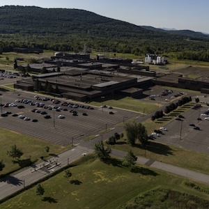
Deca Technologies announced the signing of an agreement with IBM to implement Deca’s M-Series™ and Adaptive Patterning® technologies in IBM’s advanced packaging facility in Bromont, Quebec. Through the agreement, IBM will implement a high-volume manufacturing line with a focus on Deca’s M-Series Fan-out Interposer Technology (MFIT™).
This collaboration builds on IBM’s strategy to develop its advanced packaging capabilities. IBM Canada's plant in Bromont is one of North America’s largest semiconductor assembly and test sites and has been at the forefront of packaging innovation for over five decades. Recent investments to expand the site’s capabilities have positioned it as a critical hub for high-performance packaging and chiplet integration, supporting technologies like MFIT that are essential for AI, HPC, and data center applications.
Deca’s M-Series platform is the highest-volume fan-out packaging technology in the world, with over seven billion M-Series units shipped. MFIT builds on this proven foundation by integrating embedded bridge die for chips’ last processor and memory integration delivering high-density, low-latency connections between chiplets. MFIT provides a cost-effective alternative to full silicon interposers, offering improved signal integrity, greater design flexibility, and the scalable format needed for ever-larger AI, HPC, and data center devices.
This cooperation reflects the shared commitment of IBM and Deca to advance the next generation of semiconductor packaging. By combining IBM’s advanced packaging capabilities with Deca’s proven technology, the two companies are expanding the global supply chain for the future of high-performance chiplet integration and advanced computing systems.
“Advanced packaging and chiplet technology are critical for faster, more efficient computing solutions in the age of AI. Deca will help ensure IBM’s Bromont facility remains at the forefront of these innovations, strengthening our commitment to helping our clients bring products to market faster and deliver better performance for AI and data-heavy applications,” said Scott Sikorski, Head of Business Development for Chiplets & Advanced Packaging at IBM.
“IBM’s rich history in semiconductor innovation and advanced packaging makes them an ideal partner to bring MFIT to high-volume production,” said Tim Olson, Founder and CEO of Deca. “We are thrilled to be working together to bring this advanced interposer technology to the North American ecosystem.”
Share on:


Testimonial
"Our marketing partnership with I-Connect007 is already delivering. Just a day after our press release went live, we received a direct inquiry about our updated products!"
Rachael Temple - AlltematedSuggested Items
I-Connect007 Editor’s Choice: Five Must-Reads for the Week
10/31/2025 | Nolan Johnson, I-Connect007Last week, the IMPACT conference took place in Taipei, bringing together advanced packaging experts from around the globe to share their knowledge. We’ll be bringing you post-conference coverage over the next few weeks, so look for that in our newsletters, and in the Advanced Electronic Packaging Digest. Other news seemed to have the U.S. at the center of the global discussions. My picks start in Phoenix, where TSMC, NVIDIA, and Amkor are all scrambling to establish new capabilities. There’s nothing like a strong demand signal to cause build-out, and AI chips are doing exactly that.
LPKF Delivers Key Strategic Technology to Fraunhofer's Glass Panel Technology Group
10/29/2025 | LPKFLPKF Laser & Electronics SE is one of the initiators of the Glass Panel Technology Group (GPTG), a consortium encompassing the entire process chain for advanced semiconductor packaging with glass substrates.
Koh Young Unveils Breakthrough Innovations at Productronica and SEMICON Europa 2025
10/28/2025 | Koh YoungKoh Young, the industry leader in True 3D measurement-based inspection and metrology solutions, will showcase a wave of innovations at Productronica and SEMICON Europa 2025, taking place November 18–21 at Messe München, Germany.
Nvidia’s Blackwell Chips Made in Arizona Still Head to Taiwan for Final Assembly
10/27/2025 | I-Connect007 Editorial TeamNvidia has begun production of its next-generation Blackwell GPUs in the United States, but the company still depends heavily on Taiwan to complete the process, The Register reported.
YES Selected to Deliver Full Portfolio of Advanced Packaging Tools for Glass Panel AI and HPC Applications
10/24/2025 | BUSINESS WIREYield Engineering Systems (YES), a leading provider of advanced process equipment for AI and high-performance computing (HPC) semiconductor applications, announced that it has received multiple tool orders from a global leader in AI infrastructure solutions.