-

- News
- Books
Featured Books
- smt007 Magazine
Latest Issues
Current Issue
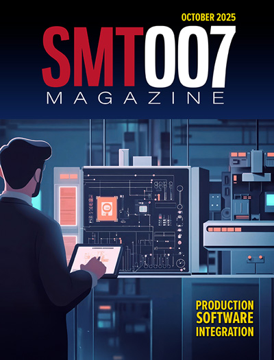
Production Software Integration
EMS companies need advanced software systems to thrive and compete. But these systems require significant effort to integrate and deploy. What is the reality, and how can we make it easier for everyone?

Spotlight on India
We invite you on a virtual tour of India’s thriving ecosystem, guided by the Global Electronics Association’s India office staff, who share their insights into the region’s growth and opportunities.

Supply Chain Strategies
A successful brand is built on strong customer relationships—anchored by a well-orchestrated supply chain at its core. This month, we look at how managing your supply chain directly influences customer perception.
- Articles
- Columns
- Links
- Media kit
||| MENU - smt007 Magazine
Be the Partner Engineers Can Rely On
July 8, 2025 | Nolan Johnson, SMT007 MagazineEstimated reading time: 1 minute
Green Circuits’ unique niche in the electronics manufacturing industry comes partly from its location in Silicon Valley, but also from its specialty of serving up quick-turn prototypes and low-volume work with high-complexity production. In this conversation, CEO Michael Hinshaw emphasizes the value of end-to-end services, especially while the pace of R&D development is accelerating amidst a growing demand for complexity across industries. Green Circuits’ sustained success, he says, stems from being a partner engineers can rely on—something that scales through relationships, referrals, and a reputation for complex builds.
Nolan Johnson: Your location in Silicon Valley provides a unique placement and customer base to serve locally. How do you describe your niche at Green Circuits?
Michael Hinshaw: To our customers, we are a quick-turn prototype house, but we straddle the line between the capabilities of a large contract manufacturer (CM) and the agility and interpersonal relationships of a small shop. Truthfully, with 190 employees, we're probably one of the largest CMs—certainly one of the largest quick-turn CMs—in California, and maybe even in the U.S. We run five lines with 20 Juki machines, so our lines are substantial. Our builds focus on agility and high complexity. We've can take customers from prototype into low-volume complex production.
Silicon Valley is a solid customer base for us. I'd say about 60% of what we do is on the West Coast; 40% is in the rest of the country, including New England; Space Coast (Florida); Huntsville, Alabama; Texas; and Colorado. We've a diverse geographic footprint.
Our customer mix is about 30% aerospace and defense and about 30% medical. The rest is a mix of power systems, automation, and AI, all with a tendency toward higher complexity, smaller volumes, and high-performance situations.
To continue reading this interview, which originally appeared in the July 2025 SMT007 Magazine, click here.
Testimonial
"Advertising in PCB007 Magazine has been a great way to showcase our bare board testers to the right audience. The I-Connect007 team makes the process smooth and professional. We’re proud to be featured in such a trusted publication."
Klaus Koziol - atgSuggested Items
Avnet Technology Links STMicroelectronics’ STM32 Microcontrollers
04/11/2025 | AvnetDesign engineers who struggle with chip down design will now be able to quickly prototype and deploy their projects based on STM32 series of microcontrollers, specifically the STM32F7 and STM32N6 series.
EDA Tools and the Designer of the Future
01/28/2025 | Andy Shaughnessy, Design007 MagazineWe’re seeing new, young technologists moving into the PCB design and design engineering segment, and it’s just in time; many veteran designers are headed to retirement. At the same time, there have been various recent advances in EDA tools. What will the PCB designer’s job—and the designer’s software tools—look like in the next five years? Bob Potock, vice president of marketing for Zuken USA, weighs in on the PCB designers of tomorrow, and the EDA tools that will take them into an evermore complex future.
Designers Notebook: Implementing HDI and UHDI Circuit Board Technology
10/23/2024 | Vern Solberg -- Column: Designer's NotebookTo accommodate new generations of high I/O semiconductor packaging, circuit board technology has undergone significant changes in both the fabrication process method and the criteria for base material selection. The reason behind these changes is the new high-function semiconductor package families that require more terminals than their predecessors and a significantly narrower terminal pitch.
The Many Complexities of PFAS
03/26/2024 | Marcy LaRont, PCB007 MagazineIn its simplest definition, PFAS is a group of chemicals used to make fluoropolymer coatings and products that resist heat, oil, stains, grease, and water. Fluoropolymer coatings can be in a variety of products. Though this definition is not inaccurate, it can be misleading. Depending on who you ask, there are upward of 10,000 PFAS chemistries that can meet various definitions.
IPC White Paper Emphasizes Critical Importance of Data Analytics for Electronics Manufacturing Process
02/26/2024 | IPCThe increasing complexity of electronics manufacturing requires embracing data analytics to manage electronics factories, according to a new white paper from IPC’s Chief Technologist Council (CTC), "Outlook for Data Analytics in the Electronics Manufacturing Industry."


