


 It’s Only Common Sense: If You’re Not Differentiated, You’re Dead
 Alpha Insights, Performance by Design: The Future of PCB Manufacturing in the Midwest
 Happy’s Tech Talk #43: Engineering Statistics Training With Free Software


Koh Young Highlighting Dimensional Metrology & Inspection Solutions at the Binghamton University Electronics Packaging Symposium
August 12, 2025 | Koh YoungEstimated reading time: 1 minute
Koh Young, the industry leader in True 3D™ measurement-based dimensional metrology and inspection solutions, is proud to announce its sponsorship and participation in the 36th Annual Electronics Packaging Symposium (EPS), hosted at the GE Aerospace Research Campus in Niskayuna, New York, on September 03-04, 2025. Organized by the Binghamton University Integrated Electronics Engineering Center (IEEC), EPS brings together thought leaders from industry, academia, and government to share the latest advances in electronic packaging, assembly, and reliability.
The two-day program will feature keynote addresses, technical sessions, and panel discussions covering heterogeneous integration, advanced materials, system reliability, thermal management, and additive manufacturing. Attendees will gain insight into emerging trends and manufacturing challenges across defense, aerospace, automotive, semiconductor, and high-performance computing applications.
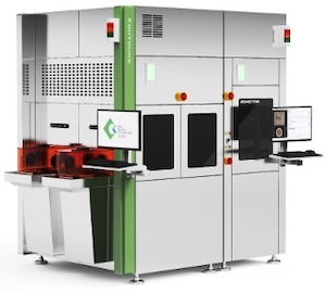
As an exhibitor, Koh Young will showcase how its AI-powered True 3D dimensional metrology and inspection solutions are helping manufacturers meet the exacting demands of advanced packaging and semiconductor processes. From wafer-level to system-in-package measurement, Koh Young’s technology delivers accurate, repeatable data that enables smarter process control, higher yields, and zero-defect production goals.
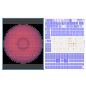
Dimensional Metrology for Advanced Packaging
Koh Young’s Meister Series is engineered specifically for advanced packaging applications such as system-in-package (SiP), wafer-level packaging (WLP), and die stacking. These systems provide ultra-high-resolution inspection capabilities to handle the smallest features and tightest tolerances in next-generation designs. Complementing the Meister series, ZenStar delivers wafer-level dimensional metrology to detect and measure critical parameters at the earliest possible stage, ensuring that only known-good components move forward in the process. Together, these solutions help manufacturers maintain tight process windows, improve yield, and reduce costly rework.
“Advanced packaging technologies are driving rapid innovation in electronics manufacturing, but they also introduce new complexities in process control and quality assurance,” said Joel Scutchfield, General Manager at Koh Young Ameria. “EPS offers a valuable opportunity to connect with engineers, researchers, and decision makers to demonstrate how our True 3D solutions can help them overcome these challenges and accelerate innovation.”
In addition to networking with attendees, Koh Young will be available to discuss real-world case studies and technology roadmaps that address next-generation packaging needs. The exhibition floor will provide a hands-on look at the tools and solutions shaping the future of electronics manufacturing.
Share on:


Testimonial
"We’re proud to call I-Connect007 a trusted partner. Their innovative approach and industry insight made our podcast collaboration a success by connecting us with the right audience and delivering real results."
Julia McCaffrey - NCAB GroupSuggested Items
Interposers, Substrates, and Advanced Manufacturing
10/13/2025 | Marcy LaRont, I-Connect007I attend a lot of industry trade shows and conferences. Lately, during conversations with technologists, I’ve noticed that there is some confusion about what exactly constitutes an interposer. One question I hear every so often is, “Are all interposers substrates?” The short answer to that question is no. But some interposers are, in fact, full substrates.
I-Connect007 Editor’s Choice: Five Must-Reads for the Week
10/10/2025 | Nolan Johnson, I-Connect007I-Connect007 has a new monthly digest newsletter, the Advanced Electronic Packaging Digest, and as I was scanning our advanced packaging newsfeeds this week, I came across a primer from tokenring.ai (republished through station WRAL, Raleigh, North Carolina), which I found quite useful. Whether you’re a designer, fabricator, or assembler, the package schemes being developed will change how you work, so be sure to keep your eye on the technological horizon and subscribe to the monthly Advanced Electronic Packaging Digest.
The Latest Issue: Advanced Electronics Packaging Digest to Explore Critical Minerals, Substrates, and Reliability Standards Driving Next-Gen Electronics
10/09/2025 | I-Connect007I-Connect007 is pleased to announce the upcoming issue of Advanced Electronics Packaging Digest (AEPD) on October 13, 2025, featuring expert insights on the technologies shaping the future of advanced packaging. As the electronics industry evolves, this issue takes a closer look at the materials, designs, and standards redefining performance and reliability across global markets.
Circular Packaging Market to Reach $98.0 Billion by 2035
10/08/2025 | Fact.MRThe market's journey from USD 45.8 billion in 2025 to USD 98.0 billion by 2035 represents substantial growth, the market will rise at a CAGR of 7.9% demonstrating the accelerating adoption of sustainable packaging systems and circular economy solutions across food & beverage, personal care, and e-commerce sectors.
Amkor Technology Breaks Ground on New Semiconductor Advanced Packaging and Test Campus in Arizona
10/08/2025 | Amkor TechnologyAmkor Technology, Inc., a leading provider of semiconductor packaging and test services, in collaboration with the Trump Administration, announces the groundbreaking and expanded planned investment of its new state-of-the-art outsourced semiconductor advanced packaging and test campus in Arizona.