


 It’s Only Common Sense: Creativity Is Noisy, Messy, and So Worth It
 Dan’s Biz Bookshelf: ‘The Soul of a New Machine’


Semiconductor industry experts will convene at SEMICON Europa 2025, November 18-21 at Messe München in Munich, to explore the latest trends and innovations in advanced packaging and fab management. The Advanced Packaging Conference (APC), Fab Management Forum (FMF) and MEMS and Imaging Sensors Summit (MEMS) at SEMICON Europa will each focus on driving sustainable solutions to meet the evolving demands of the semiconductor market. Co-located with productronica, SEMICON Europa is the region’s premier event connecting the entire electronics design and manufacturing supply chain. Registration is open for APC, FMF, and MEMS.
“Global collaboration is of strategic importance to advancing Europe’s economic resilience and competitiveness,” said Laith Altimime, President of SEMI Europe. “The Advanced Packaging Conference, Fab Management Forum, and MEMS and Imaging Sensors Summit provide critical platforms for bringing together industry experts, innovators, and decision makers to ensure continued and sustainable growth throughout the European microelectronics supply chain.”
“We are entering a pivotal era where AI demands a radical rethinking of hardware innovation. At imec, we believe Europe’s strength lies in its ability to align research, industry, and policy around shared semiconductor roadmaps,” said Luc Van den hove, President and CEO of imec. “Our collaborative efforts, such as the NanoIC pilot line and our joint high NA EUV lithography research lab, demonstrate how collaboration can accelerate technology innovation to advance the development and adoption of next-generation technologies that impact industries on a broader scale. SEMICON Europa offers a unique opportunity to spotlight how collaborative innovation is shaping Europe’s semiconductor future—strengthening our competitiveness and reinforcing leadership across the entire value chain.”
Advanced Packaging Conference
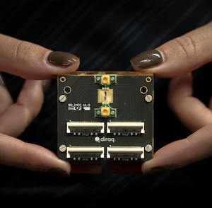
Advanced Packaging: Key Enabler for System Performance
The APC will spotlight innovations such as 2.5D and 3D stacking, chiplet integration, and heterogeneous packaging that are driving next-generation electronics. By improving power efficiency, thermal management, and system performance while enabling breakthroughs in high-performance computing and AI, advanced packaging is proving to be a critical enabler of superior performance, energy efficiency, and reliability.
This year’s APC will focus on:
- Market Insights in an Evolving Geopolitical Landscape
- Advanced Materials and Processes for Wafer- and Panel-Level Packaging
- Packaging Innovations for Silicon Photonics
- Reliability and Yield Optimization with Digital Twin and AI
- Advances in Testing, Inspection, and Metrology
Speakers include experts from 3D-Micromac AG, Advantest Europe, BESI Austria GmbH, Comet, Dassault Systèmes, DELO Industrial Adhesives, ESPAT-Consulting, Excillum AB, Fraunhofer IZM, GlobalFoundries, Henkel Electronic Materials, imec VZW, Lam Research, Lidrotec GmbH, NXP Semiconductors, Onto Innovation, RoodMicrotec GmbH, Shellback Semiconductor Equipment, and Siemens EDA.
Fab Management Forum
Europe’s Fab Resilience Through Collaboration
Collaborative innovation can strengthen Europe’s semiconductor manufacturing ecosystem. This year’s FMF will feature discussions on strategies to enhance fab efficiency and performance through cutting-edge technologies while maintaining sustainability. Attendees will gain insights into fostering partnerships that drive both competitiveness and long-term sustainability in semiconductor production.
FMF topics will focus on:
- Competitive Fab Strategies for Europe
- Collaboration for European Supply Chain Resilience
- Smart Factories Powered by Automation and AI
- Disruptive Technologies Reshaping Fabs
Speakers include experts from ACCRETECH, Air Liquide, Bosch, Comet, Dorfner Anzaplan GmbH, Inficon, Infineon Technologies, Neura Robotics, Nippon Gases, Planimize, Semilab, SEMI, Siemens, STMicroelectronics, Swansea University, and X-Fab.


