


 Fresh PCB Concepts: Resilience and Renewal in Domestic PCB Manufacturing
 Designers Notebook: Power and Ground Distribution Basics
 Elementary, Mr. Watson: Heat—The Hidden Villain of Power Electronics


Thallner Recognized for Leadership and Innovation in Semiconductor Equipment and MEMS Manufacturing
October 10, 2025 | SEMIEstimated reading time: 2 minutes
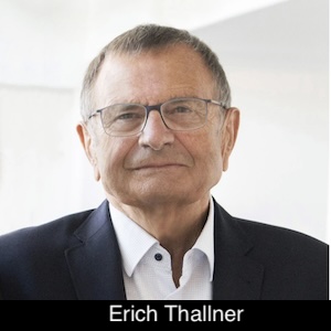
SEMI, the industry association serving the global semiconductor and electronics design and manufacturing supply chain, announced Erich Thallner, President and Co-founder of EV Group (EVG), as its first SEMI Americas Catalyst Award recipient at SEMICON West 2025. This new award will be presented annually to individuals and organizations whose visionary leadership, technical excellence, and collaborative nature have uplifted the semiconductor industry.
Since founding EVG in 1980, Thallner has been instrumental in perfecting the company’s tight product development process, resulting in numerous innovations that have transformed the global industry. His consistent and strategic R&D investments have also positioned the company to quickly transition products from development and small-scale manufacturing to high-volume production.
“Several important technologies would not have been realized without Erich's forward-thinking leadership,” said Joe Stockunas, President of SEMI Americas. “In an industry that constantly requires new innovations to keep up with rising chip demand, Erich’s commitment and ability to spot trends early have been fundamental for industry-wide advancement. SEMI is proud to honor Erich as our first SEMI Americas Catalyst Award recipient – his 45 years of dedicated industry service have set the bar high.”
Thallner Thallner has led EVG to multiple groundbreaking and original discoveries, including the first double-sided mask aligner for MEMS commercialization, the first temporary bonding and debonding solution, and the first automated wafer bonding system for 300-mm wafers, among several others.
Additionally, Thallner played a pivotal role in establishing EVG’s presence in the United States. Headquartered in St. Florian am Inn, Austria, the company brought its sales, technical equipment support, and process services to Arizona in 1994, decades before most others would follow suit. EVG has since expanded its North American presence to both Oregon and New Mexico and aligned with Arizona State University to support its Flexible Electronics and Display Center (FEDC).
“I am deeply honored to accept the SEMI Americas Catalyst Award,” said Erich Thallner. “As a long-standing SEMI member, EVG shares the goals of this leading industry association to help the semiconductor supply chain members grow their business and address top challenges worldwide. In line with our Triple-i philosophy of ‘invent - innovate – implement’, we enable our customers, including our strategic partners in North America, to successfully realize their product ideas. Our North America subsidiary has played a pivotal role in this effort for more than 30 years.”
Share on:


Testimonial
"In a year when every marketing dollar mattered, I chose to keep I-Connect007 in our 2025 plan. Their commitment to high-quality, insightful content aligns with Koh Young’s values and helps readers navigate a changing industry. "
Brent Fischthal - Koh YoungSuggested Items
Kulicke and Soffa Industries Announces CEO Transition
10/30/2025 | PRNewswireKulicke and Soffa Industries, Inc. announced that Dr. Fusen Chen has agreed to retire from his position as President and CEO, and as a member of the Board, effective December 1, 2025, due to health reasons.
SEMI Reports Global Silicon Wafer Shipments to Rebound 5.4% in 2025, with New Record Expected by 2028
10/30/2025 | SEMIGlobal shipments of silicon wafers are projected to increase 5.4% in 2025 to 12,824 million square inches (MSI) followed by steady growth through 2028 when the market is expected to reach a new industry record of 15,485 MSI, SEMI reported in its annual silicon shipment forecast.
Delta to Acquire Noda RF Technologies to Enhance its Power Solutions Portfolio for the Semiconductor Industry
10/30/2025 | PRNewswireDelta Electronics, Inc., a leader in power management and smart green solutions, today announced the acquisition of 90.23% stake of Japan's Noda RF Technologies Co., Ltd. (NRF) through its subsidiary Delta Electronics (Netherlands) B.V. for JPY 5,024 million (approximately NT$1,034 million).
LPKF Delivers Key Strategic Technology to Fraunhofer's Glass Panel Technology Group
10/29/2025 | LPKFLPKF Laser & Electronics SE is one of the initiators of the Glass Panel Technology Group (GPTG), a consortium encompassing the entire process chain for advanced semiconductor packaging with glass substrates.
SEMI Reports Global Silicon Wafer Shipments to Rebound 5.4% in 2025, with New Record Expected by 2028
10/29/2025 | SEMIGlobal shipments of silicon wafers are projected to increase 5.4% in 2025 to 12,824 million square inches (MSI) followed by steady growth through 2028 when the market is expected to reach a new industry record of 15,485 MSI, SEMI reported today in its annual silicon shipment forecast.