


 Powering the Future: Why Thermal Management Defines the Future of Electronics
 Standard of Excellence: Engineering Is the New Sales—How Technical Collaboration Wins Business
 SMT Perspectives & Prospects: Artificial Intelligence, Part 7—Data Module 2


Imec Launches 300mm GaN Program to Develop Advanced Power Devices and Reduce Manufacturing Costs
October 13, 2025 | ImecEstimated reading time: 2 minutes
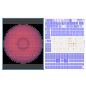
Imec, a world-leading research and innovation hub in nanoelectronics and digital technologies, welcomes AIXTRON, GlobalFoundries, KLA Corporation, Synopsys, and Veeco as first partners in its 300mm gallium-nitride (GaN) open innovation program track for low- and high-voltage power electronics applications. This program track, part of imec’s industrial affiliation program (IIAP) on GaN power electronics, has been set up to develop 300mm GaN epi growth, and low and high voltage GaN high electron mobility transistor (HEMT) process flows. The use of 300mm substrates will not only reduce GaN device manufacturing costs, but it will also allow the development of more advanced power electronics devices, such as efficient low-voltage point-of-load converters for CPUs and GPUs.
The recent market introduction of GaN-based fast battery chargers underscores the potential of GaN technology for power electronics applications. Backed by continuing progress made in GaN epi growth, GaN device and IC manufacturing, reliability and robustness, and system-level optimization, GaN technology is poised to enable a new generation of power electronics products.
These will enter the market with reduced form factors, smaller weight, and superior energy conversion efficiency compared to Si-based solutions. Examples are on-board chargers and DC/DC converters for automotive applications, inverters for solar panels, and power distribution systems for telecom and AI data centers – where GaN-based building blocks contribute to the overall decarbonization, electrification and digitalization of society.
A notable trend in GaN technology development is the move to larger wafer diameters, with capacity now mostly available on 200mm. With the launch of its 300mm GaN program track, imec is taking the next step, building on its 200mm expertise.
Stefaan Decoutere, fellow and program director of the GaN power electronics program at imec: “The benefits of transitioning to 300mm wafers go beyond upscaling production and reducing manufacturing costs. Our CMOS-compatible GaN technology now has access to 300mm state-of-the-art equipment that will allow us to develop more advanced GaN-based power devices. Examples are aggressively scaled low-voltage p-GaN gate HEMTs for use in point-of-load converters, supporting energy-efficient power distribution for CPUs and GPUs.”
As part of the 300mm GaN program, a baseline lateral p-GaN HEMT technology platform will first be established for low-voltage applications (100V and beyond), using 300mm Si(111) as a substrate. For this, process module work centered around p-GaN etch and Ohmic contact formation is ongoing. Later, high-voltage applications are targeted. For 650V and above, developments will utilize 300mm semi-spec and CMOS-compatible QST® engineered substrates (a material with poly-crystalline AlN core). During the developments, control over the bow of the 300mm wafers, and their mechanical strength are prime concerns.
The launch of the 300mm GaN program follows successful 300mm wafer handling tests and mask set development. Imec expects to have full 300mm capabilities installed in its 300mm cleanroom by the end of 2025.
“The success of the 300mm GaN development also hinges on the ability to establish a robust ecosystem and jointly drive innovation from 300mm GaN growth and process integration to packaging solutions,” adds Stefaan Decoutere. “We are therefore pleased to announce AIXTRON, GlobalFoundries, KLA Corporation, Synopsys, and Veeco as first partners in our open R&D program track on 300mm GaN and hope to welcome more partners soon. Because developing advanced GaN power electronics requires close coupling between design, epitaxy, process integration, and applications – a coupling that has proved to be critical for our pioneering work on 200mm GaN.”
Share on:


Testimonial
"Your magazines are a great platform for people to exchange knowledge. Thank you for the work that you do."
Simon Khesin - Schmoll MaschinenSuggested Items
Learning with Leo: Why Risk-based Auditing Is Reshaping Cable Assembly Quality
04/01/2026 | Leo Lambert -- Column: Learning With LeoEffective product development requires early and active participation from all stakeholders. The design process must include input from supply chain, manufacturing engineering, purchasing, quality, and production. A design cannot be considered complete until it has been evaluated against the full manufacturing process, whether executed by an OEM or a subcontractor. Without this collaboration, designs are often released that are not manufacturable in real-world conditions.
Foxconn Joins Global DEI Initiative to Promote Diversified and Integrated Talent Governance
03/24/2026 | FoxconnFoxconn Technology Group has chosen to join the CommonWealth DEI initiative, hoping to exchange diverse, equal, and inclusive practical experiences with more companies through an open platform, and to promote talent sustainability from an internal governance issue of a single company to an action for common learning and dialogue across the industry.
Dongguk University Develops Breakthrough Material for Next-Gen Smart Devices
03/13/2026 | PRNewswireNext-generation optoelectronic systems (devices that convert light to electrical energy) leverage organic semiconductor-based indoor energy-autonomous architectures for cutting-edge applications.
Myrias Optics Secures $2.1M Seed Funding to Advance Wafer-Level Metaoptics
02/25/2026 | PRNewswireMyrias Optics, a world leader in wafer-level metaoptics and diffractive optical technologies, announced the closing of a $2.1 million Seed 1 financing round in January 2026.
EPC Signs Strategic GaN Licensing and Second-Source Deal with Renesas
02/16/2026 | PRNewswireEfficient Power Conversion (EPC), the world leader in enhancement-mode gallium nitride (eGaN®) power devices, announced a comprehensive licensing agreement with Renesas Electronics Corporation, a premier global supplier of advanced semiconductor solutions and high-voltage GaN transistors.